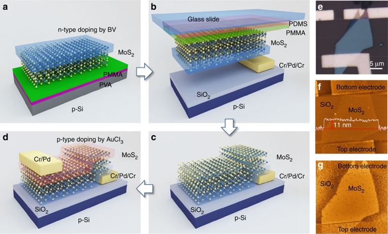
Figure 1. Fabrication of chemically doped vertical p–n homogeneous junction in a few-layer MoS2 flake.
(a) A MoS2 flake was transferred on a PMMA/PVA/Si substrate, and then BV-doped and annealed. (b) After dissolving the PVA layer in deionized water, the PMMA film supporting a MoS2 flake was transferred to a PDMS/glass substrate. (c) The MoS2 flake was stamped on the SiO2/Si substrate, and the n-doped surface was aligned with the Cr/Pd/Cr bottom electrode prepared in advance. (d) After AuCl3 doping and annealing, the vertical p–n junction in the MoS2 flake was formed, followed by the deposition of a Cr/Pd top electrode. (e–g) Optical microscopy image, AFM height image with a line scan profile, and AFM phase image of a vertical p–n homogeneous junction composed of a few-layer MoS2 flake.

