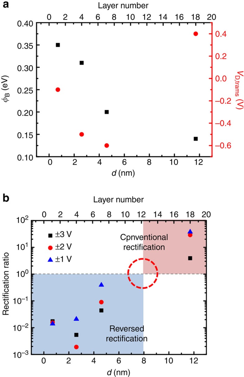
Figure 6. Schottky barrier height, transition drain voltage and rectification ratio depending on the thickness of MoS2.
(a) The barrier height and DT–FNT transition voltage as functions of the MoS2 thickness and layer number. (b) Current rectification ratio as a function of the MoS2 thickness and layer number at various VD (±3, ±2 and ±1 V) levels, indicating a transition between the conventional rectification and reversed rectification at ~8 nm (red dot circle).

