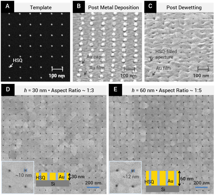
Figure 2. Experimental results showing the template-guided metal dewetting process.
(A) SEM image of HSQ defined nanopillars on bare silicon. Periodicity of nanopillars = 100 nm. (B) Tilted SEM image of sample after metal deposition. (C) Tilted SEM image of nano-apertures obtained after thermally induced dewetting. The grain sizes increased significantly after thermal treatment. (D) SEM micrograph of nanoaperture array in 30 nm thick film obtained over a ~1.5 μm by 1.5 μm area. Scale bar: 200 nm. (E) SEM micrograph of nanoaperture array in 60 nm thick film obtained over a ~1.5 μm by 1.5 μm area. (D & E - insets) High magnification SEM images showing a close-up of the nanoapertures in D and E respectively.

