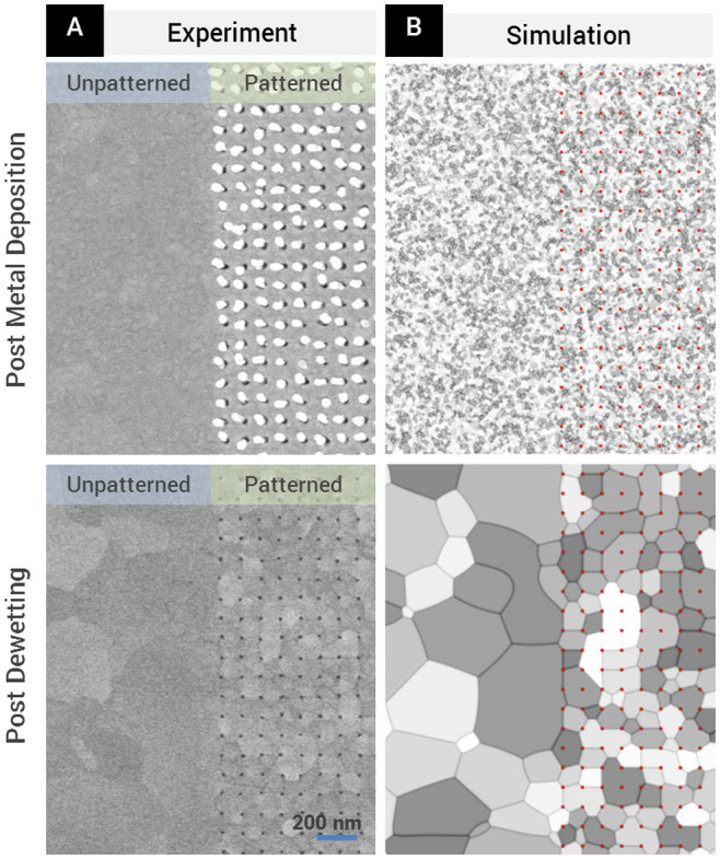
Figure 3. Patterned area versus an unpatterned area before and after dewetting.

(A) SEM micrograph of samples with gold film thicknesses of 60 nm, and nanoaperture periodicity of 100 nm. Thermal annealing induces recrystallization of the metal, with noticeable grain-boundary pinning yielding smaller grain sizes in the patterned versus the unpatterned areas. (B) In the simulation results, red dots indicate positions of the nanopillars (with gold caps) and nanoapertures before and after dewetting respectively. The simulation results agree with the experimental findings, showing the overall increase in grain sizes after dewetting, and grain-boundary pinning in the patterned areas resulting in smaller grain sizes as compared to unpatterned areas.
