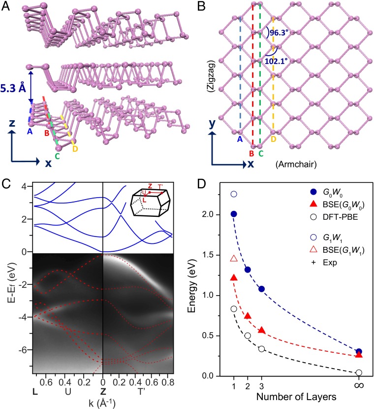
Fig. 1.
Crystal structure and band structure of black P. (A) Side view of the black P crystal lattice. The interlayer spacing is 0.53 nm. (B) Top view of the lattice of single-layer black P. The bond angles are shown. The corresponding x, y, and z directions are indicated in both A and B. x and y correspond to the armchair and zigzag directions of black P, respectively. (C) Band structure of bulk black P mapped out by ARPES measurements. A band gap around 0.3 eV is clearly observed. Superimposed on top are the calculated bands of the bulk crystal. Blue solid and red dashed lines denote empty and filled bands, respectively. The directions of the ARPES mapping are along U (L–Z) and T′, as indicated in the first Brillion zone shown in Inset. Ef is the Fermi energy (1). (D) The evolution of the band gap calculated by different methods, and the energy of the optical absorption peak according to the stacking layer number of few-layer black P (31). C and D are reproduced with permission from refs. 1 and 31, respectively.

