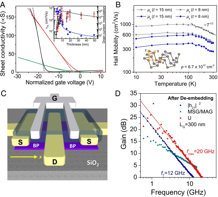
Fig. 4.
Electronic properties of black P thin film. (A) Sheet conductivity measured as a function of gate voltage for devices with different thicknesses: 10 nm (black solid line), 8 nm (red solid line), and 5 nm (green solid line), with field-effect mobility values of 984 cm2⋅V−1⋅s−1, 197 cm2⋅V−1⋅s−1, and 55 cm2⋅V−1⋅s−1, respectively. (Inset) Field-effect mobilities were extracted from the line fit of the linear region of the conductivity (dashed lines). A is reproduced with permission from ref. 1. (B) Angle-resolved Hall mobility vs. temperature. (Inset) Schematic view of a single-layer black P showing different crystalline directions. B is reproduced with permission from ref. 2. (C) Schematic of the black P transistor device structure. (D) Current and power gain in black P transistors at gigahertz frequency. Shown are the short-circuit current gain h21, maximum stable gain (MSG)/maximum available gain (MAG), and unilateral power gain U of the 300-nm channel length device after de-embedding. C and D are reproduced with permission from ref. 58.

