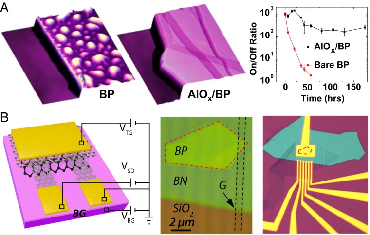
Fig. 6.
Protective encapsulation of black P material and devices. (A) AFM images and on–off ratio of black P thin film FETs without and with AlOx overlayer protection vs. ambient exposure time. A is reproduced with permission from ref. 53. (B) Schematic and optical micrograph of a graphene-contacted black P device with boron nitride encapsulation. Red and black dashed areas (Center) show the black phosphorus crystal and one of the graphene strips, respectively. The BN encapsulation layer is also shown. B is reproduced with permission from ref. 94.

