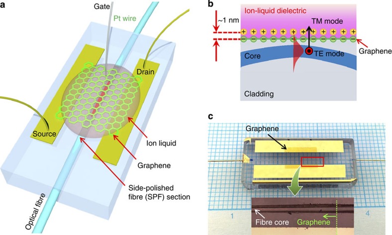
Figure 1. Schematic view and images of gate-controlled all-fibre graphene devices.
(a) Schematic diagram of gate-variable all-fibre graphene device. The SPF was fabricated using a standard single-mode optical fibre (SMF-28e) where two metal electrodes were deposited with 50-nm thickness at both sides of the side-polished region. After transferring the graphene layer, ion liquid was applied to the graphene. Two electrodes and a Pt wire were used as source, drain and gate, respectively. The electrical transport property as a function of applied gate voltages was monitored through the measurement of ID. Optical power in the fibre was measured using a laser diode at 1,550 nm, an in-line polarization controller and an optical power metre. (b) Schematic of side view of the all-fibre graphene devices. The field tail of the guided mode interacts with the graphene. Ion liquid acts as the gate medium as well as a transparent cladding that enhances the field strength at the graphene surface. The applied gate voltage makes the ion form an EDL between the ion liquid and graphene with a thickness of about 1 nm, which efficiently modifies the Fermi level in graphene. (c) Optical image of the fabricated device without ion liquid. The graphene sheet (7 × 5 mm2) covers the region of interaction with the fibre (∼5 mm). Inset: microscope image of side-polished surface where red light was launched from fibre end to visualize the core at polished surface.

