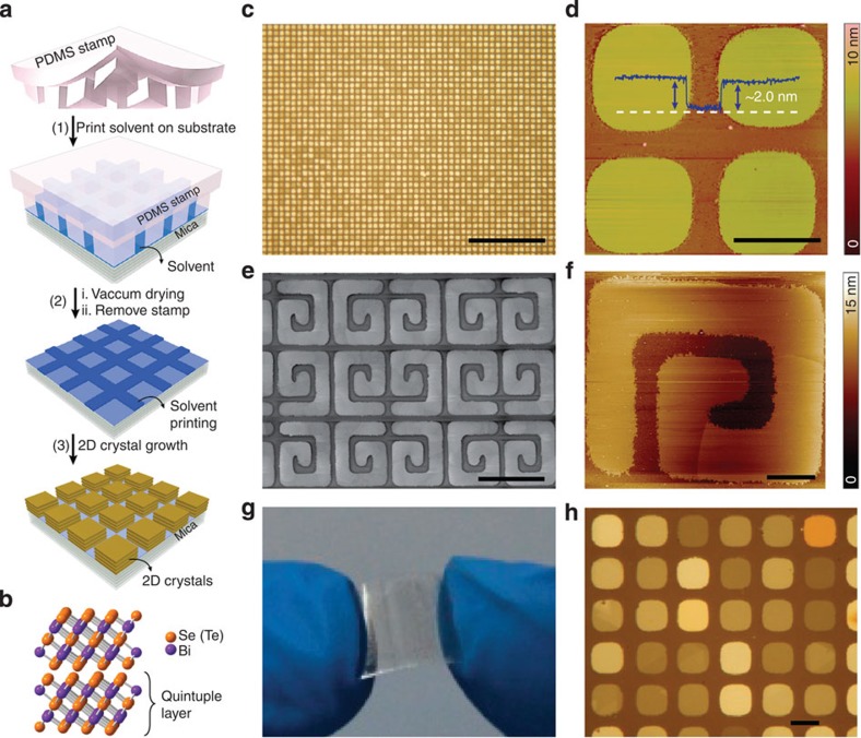
Figure 1. Patterning of 2D chalcogenide crystals.
(a) Schematic representation of procedures for patterning of 2D chalcogenide crystals. (b) Layered crystal structure of chalcogenide topological insulators Bi2X3 (X=Se, Te), which consist of QLs. (c) Typical reflection-mode OM image of large-area 2D Bi2Se3 crystal array patterned on mica substrate. Scale bar, 200 μm. (d) AFM image of a 2 × 2 Bi2Se3 crystal array with a uniform thickness of 2 nm. Scale bar, 10 μm. (e) Scanning electron microscopy image of an array of spiral Bi2Se3 crystals. Scale bar, 50 μm. (f) AFM image of a spiral Bi2Se3 crystal. Scale bar, 10 μm. (g) Photograph of a mica substrate after patterning of 2D Bi2Se3 crystals that contains more than 200,000 crystals. (h) Typical reflection-mode OM image of 2D In2Se3 crystal array patterned on mica substrate. Scale bar, 10 μm.

