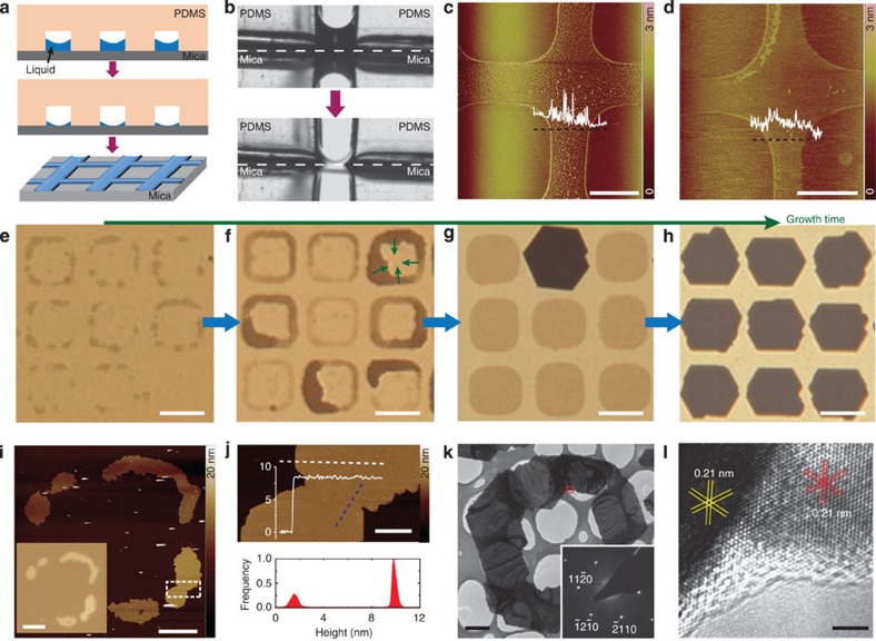
Figure 2. Mechanism of patterning 2D chalcogenide crystals.
(a) Schematic of microintaglio printing process to form imprints on mica surface. (b) Charge-coupled device camera photos showing the transfer of solvent ink from a microwell of PDMS stamp onto mica. (c,d) AFM images of the imprints on mica surface captured directly after microintaglio printing (c) and after heating at 700 °C for 1 h (d). Scale bars in c and d, 5 μm. (e–h) Transmission-mode OM images of Bi2Se3 crystals on mica at different nucleation and growth stages: the nucleation of Bi2Se3 crystal islands starting from the edge of the imprints (e), epitaxial growth of Bi2Se3 crystal ring from the edge to the middle (f), formation of complete patterns after merging of different islands (g), the formation of thicker, single crystals at longer growth time (h). Scale bars in e–h, 10 μm. (i) AFM image of a patterned Bi2Se3 crystal in the middle stage of the growth process. Scale bar, 3 μm. Inset of i: reflection-mode OM image of the same crystal. Scale bar of i inset, 5 μm. (j) Enlarged AFM image of the merging region of two domains indicated in the box of i. Scale bar, 500 nm. Below panel of j: height distribution diagram of the indicated area. (k) TEM image of a patterned Bi2Se3 crystal in the middle stage of the growth process. Scale bar, 2 μm. Inset of k: diffraction pattern of the common merged area indicated by a red square showing single-crystal nature. (l) HRTEM image from the merging region indicated in k. Scale bar, 2 nm.

