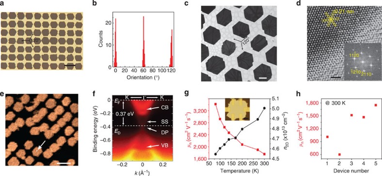
Figure 3. Evaluation of the crystal structure and electronic structure of 2D chalcogenide crystal arrays.
(a) Typical transmission-mode OM image of 7 × 10 Bi2Se3 nanoplate array with the same orientation on a transparent mica substrate. Scale bar, 20 μm. (b) Histogram of the orientation distribution of Bi2Se3 nanoplates in a. (c) TEM image of a patterned Bi2Se3 crystal array transferred to a lacey carbon support film on a TEM copper grid. Scale bar, 5 μm. (d) HRTEM image obtained from the same Bi2Se3 crystal array, with corresponding fast Fourier transformation pattern shown in the inset. Scale bar, 1 nm. (e) Full valance spectra contrast map of a 2D Bi2Se3 crystal array measured by micro-ARPES with beam spot size of <1 μm and a 1-μm step scan. Scale bar, 20 μm. (f) Electronic band structure of individual Bi2Se3 crystals, showing a direct bulk gap and surface states consisting of a single Dirac cone, a hallmark of the topological insulator. The conduction band (CB), valence band (VB), surface state (SS) and Dirac point (DP) are indicated, together with the Fermi energy (EF), the energy level of Dirac point (ED) and wave vector k. (g) Hall mobility (μn) and carrier density (n2D) as a function of temperature for an individual Bi2Se3 crystal with the thickness of ∼30 nm. Inset: OM image of a Hall-bar device fabricated on an individual Bi2Se3 crystal from a 2D array. Scale bar of inset, 5 μm. (h) Statistic distribution of room temperature mobility of five devices based on the 2D Bi2Se3 crystal array, indicating high mobility and reasonable uniformity of 2D crystals.

