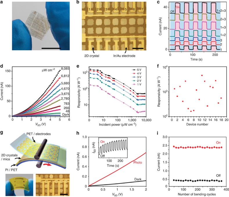
Figure 4. Electrical characterization, photodetector array and its packaged devices of patterned 2D crystals.
(a,b) Photograph and OM image of In2Se3 photodetector arrays on the transparent and flexible mica substrate. Seven channels were labelled from 1 to 7, defined by the same source. Scale bar in a, 1 cm. Scale bar in b, 20 μm. (c) Photoresponse of multiple In2Se3 photodetector channels. Source–drain voltage (VSD)=0.1 V, light power density: 4 mW cm−2. (d) Current–voltage (ISD–VSD) curves of the individual device in the dark and under different illumination intensities with a 633-nm defocused laser. (e) Dependence of photoresponse on different illumination intensities and bias voltage. The device exhibits a photoresponsivity of 1,650 A W−1 under bias of 5 V for an illumination power intensity of 622 nW cm−2 and a device area of 40 μm2. (f) Statistic distribution of photoresponsivity of 18 devices based on the semiconducting In2Se3 crystal array on mica substrates. (g) Schematic of device packaging, the photograph of packaged device and its OM image. Electrodes and In2Se3 were pressed together by a lamination process. Electrodes (Ti/Au, 10 nm/40 nm) were defined onto the PET films by photolithography and thermal evaporation. Scale bar, 20 μm. (h) Photoresponse characterization of the packaged device. Inset: time-dependent photocurrent response of the packaged In2Se3 device at a bias voltage of 5 V. (i) Current as a function of bending cycles (before/after bending to a 10 mm radius) of the packaged In2Se3 devices on mica protected by PET with the laser on or off at a bias voltage of 5 V.

