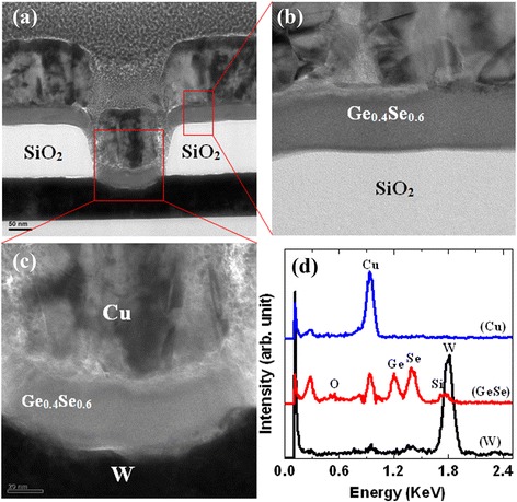
Figure 1.

TEM images and EDX analysis of a Cu/Ge0.4Se0.6/W pristine memory device. (a) TEM image of a Cu/Ge0.4Se0.6/W pristine memory device with a scale bar of 50 nm. The Ge0.4Se0.6 film shows to be amorphous, as shown in the (b) outside and (c) inside of the via-hole region. (c) Different layers are clearly shown by the dark-field TEM image and (d) corresponding EDX analysis of the W, Ge0.4Se0.6, and Cu films from (a) [33].
