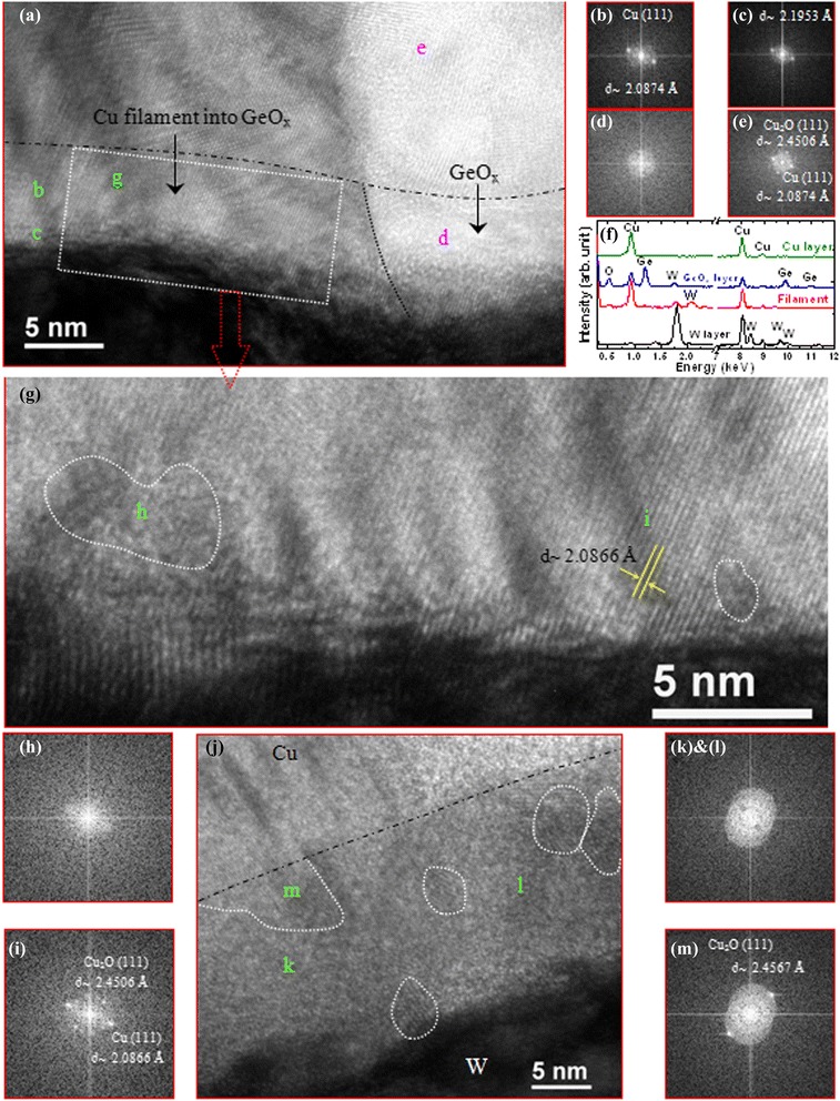
Figure 21.

HRTEM images, FFT analysis, and EDX analysis of a Cu/GeOx/W memory structure. (a) After SET operation (CC of >100 μA), the HRTEM image of a Cu/GeOx/W memory structure. A crystalline Cu nanofilament is clearly observed in the GeOx film. The FFTs confirm the (b,g,i) Cu nanofilaments, (c) Cu/W interface, (d) GeOx layer without Cu nanofilament, and (e) Cu electrode. (f) All layers and filaments are also confirmed by EDX analysis. (h) Some amorphous regions are also observed. After the unipolar RESET operation, (j) an HRTEM image is shown. (k, l) An amorphous GeOx layer with crystalline nanograins is observed because of the Ge-rich GeOx film. (m) A small amount of Cu also remains on the Cu electrode because of higher Joule heating on the filament’s weak points [20].
