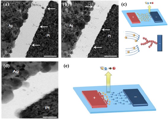
Figure 22.

TEM images and schematic diagrams for the conducting filament kinetics. (a) TEM image of a SiO2-based material after the formation of the conducting nanofilament. The arrows indicate complete and incomplete nanofilaments. The scale bar is 200 nm. (b) TEM image after RESET operation. (c) Schematic illustration of the filament growth process. (d) TEM image of a conducting filament in a-Si-based CBRAM devices. The scale bar is 50 nm. (e) Schematic diagram of the nanofilament growth process in an a-Si CBRAM device [54].
