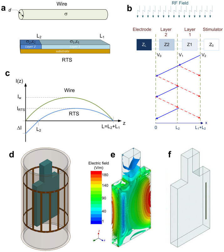
Figure 1. RTS design and simulation setup.
(a) Schematic of the PtIr wire (diameter d = 100 μm, electrical conductivity σ = 4.0·106 S/m) and the two-layer RTS design (electrical conductivity σ1 and σ2, permittivity ε1 and ε2, length L1 and L2) used for the study. (b) Equivalent circuit used to model the RTS implant with four sections: stimulator, two layer transmission line, and electrode/tissue interface. The incident RF field induces currents along the implants, which are reflected depending on neighboring sections mismatched impedance (Z0, Z1, Z2, and ZL). The resulting voltage amplitude at each interface (V0, V1, and V2) was generated by the induced current. (c) RF-induced currents along the two leads. The current in the metallic conductor forms a standing wave with high peaks in amplitude (Iw); conversely, the effect of RTS design is two-fold: a) reduces the average induced currents (IRTS) along the implant by worsening the antenna performance, and b) reduces the induced current at the electrode (ΔI) by introducing scattering within the implant. (d) CAD Model used in the numerical simulations, including a 16-leg high-pass birdcage body coil with RF shield, coil former and ASTM phantom. (e) 3 D plot of electric field magnitude at the Larmor frequency (f0 = 128 MHz) in the ASTM phantom model used in the simulations. Results were normalized to a power level yielding a whole-body SAR = 2 W/kg (i.e., Normal Operating Mode41). (f) Placement of lead inside the phantom. The location was chosen because of the high magnitude of incident electric field.

