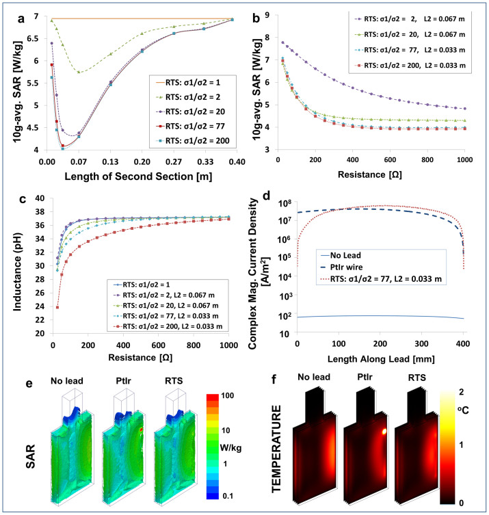
Figure 2. Optimal RTS design in phantom.
(a) 10 g-avg. SAR inside the phantom at a distance of 0.1 mm from the electrode obtained by varying the length (L2) of the second section (see Methods). Plots include different conductivity ratios for the two layers. In all cases the total resistance of the lead was R = 400 Ω. (b) 10 g-avg. SAR at the same point obtained by varying the total resistance of the lead. Plots include four combinations of conductivity ratios of the two layers and length L2 of the second section. (c) Maximum inductance of the RTS varying the total resistance of the lead. Plots include five combinations of conductivity ratios of the two layers and length L2 of the second section. (d) Amplitude of induced current inside the lead with the PtIr wire, with the RTS lead selected for prototype manufacturing (right) and in the corresponding volume of the ASTM phantom without lead. The RTS lead allowed for a 37-fold decrease in induced current at the electrode (Length along Lead = 0 mm). In all cases the total length of the leads was 40 cm. (e) Numerical simulation results at 128 MHz calculated with finite element method using the geometry shown in Fig. 1d and 1f and with either a single-electrode PtIr wire or an RTS lead. 10 g-avg. SAR in the ASTM phantom without lead (left), with the PtIr wire (middle), and with the RTS design that was selected for prototype manufacturing (right). Values were normalized to whole-body SAR of 2 W/kg. (f) Temperature maps for 15 minutes of continuous SAR exposure for the same three cases described in (e). Simulations showed that the RTS lead is transparent to the incident RF field and generated similar temperature increase (up to 0.9°C) compared with the ASTM phantom without lead. By contrast, the PtIr wire generated a temperature increase up to 12°C near the electrode (please note that the color bar threshold was set to 2°C to improve visualization.)

