
Figure 5.
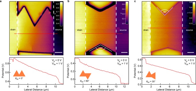
Mapping the local electrical properties across grain boundaries in large-area monolayer MoS2. (a) Local potential map (upper panel) and line scan across the red line (lower panel) showing the potential drop over the conductive channel of a biased field-effect transistor based on two merged MoS2 single crystals with the same lattice orientation. In this case, no grain boundary is expected. The smooth potential drop indicates the absence of abrupt changes of potential that would indicate the presence of an electrically resistive grain boundary. (b) Local potential map and line scan over two merged triangles with a 60° misorientation angle. This configuration is expected to result in a twin grain boundary. Its presence does not introduce an extra potential drop, indicating that it does not degrade the electrical conductivity of the material. (c) Local potential map and line scan over two merged triangles with a 30° misorientation angle. The presence of the grain boundary does not introduce an extra potential drop in the channel. Insets in line scan plots indicate relative orientations of MoS2 single crystals. Scale bars are 2 μm long.