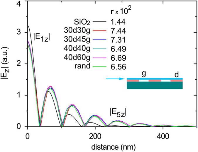
Figure 5. >Numerical simulations of GPs propagation and damping on NS-SiO2 at λ1 = 10 μm.

Inset shows a sketch of simplified 2-D model of the spacer; where d is the nano-dot size, g is the gap between neighbouring dots, and blue arrow represents the direction of the plasmon launching. The data marked with light green colour was calculated for the random geometry of the spacer (from the left to the right: d1 = 40 nm, g1 = 45 nm, d2 = 60 nm, g2 = 40 nm, d3 = 45 nm, g3 = 60 nm, d4 = 30 nm, g4 = 30 nm, d5 = 45 nm, g5 = 60 nm, d6 = 45 nm). Left-hand side axis displays an absolute value of the vertical component of electric field, taken at 3 nm distance above graphene. The damping strength r, which is defined here as a ratio between fifth and first maxima of the field (r = |E5z|/|E1z|), is given for each of calculated NS geometries in the inset of the figure.
