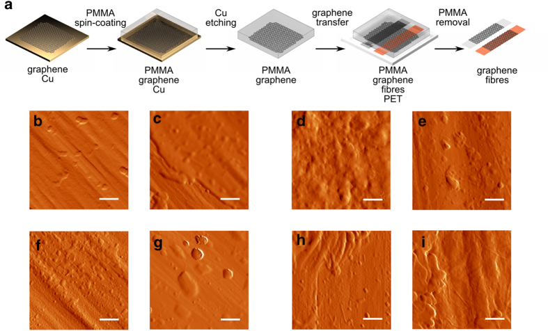
Figure 1. Graphene transfer process and AFM imaging.
(a) General graphene transfer steps: CVD growth on copper; PMMA coating; copper etching; graphene transfer to the fibers and PMMA removal. AFM amplitude images (5 × 5 μm, scale bars are 1 μm) and roughness (Ra) taken at 45° with respect to the fiber length of (b) PP (Ra = 10.3 nm); (c) PP + G (Ra = 8.3 nm); (d) PLA (Ra = 25 nm); (e) PLA + G (Ra = 12.3 nm); (f) PP UV (Ra = 8.1 nm); (g) PP UV + G (Ra = 7.7 nm); (h) PLA UV (Ra = 20.1 nm); and (i) PLA UV + G (Ra = 10.3 nm). The UV treatment makes the fibers rougher but also more homogeneous, facilitating graphene adhesion. Image (c) shows that the graphene coverage in the untreated fibers is not complete.

