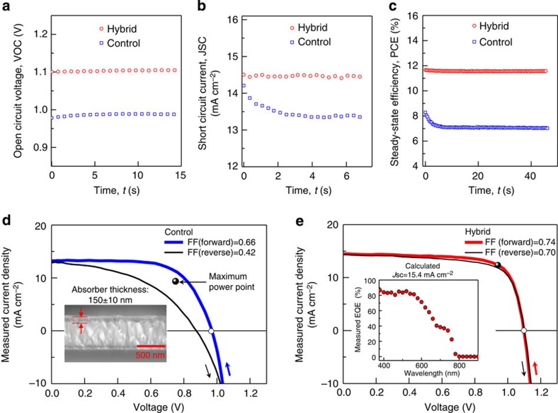
Figure 1. Steady-state photovoltaic performance of an ultrathin perovskite–PCBM hybrid film.
(a) The steady-state open-circuit voltage, VOC, (b) steady-state short circuit current density, JSC and (c) the steady-state power conversion efficiency, PCE, of perovskite–PCBM hybrid film (red) compared with the control perovskite-only film (blue). During steady-state measurement, the integrating time for each point is 0.35 s. (d) The instantaneous J–V curve of the control device (perovskite film) with high hysteresis. The thicker curve indicates forward scan starting from open-circuit condition; thin curve is the reverse scan from short circuit condition. The scanning rate is 0.2 V s−1. The fill factor (FF) of forward scan is 66% while reverse FF is reduced to 42%. The black point indicates the ‘maximum-power output point (MPP)' is measured from the steady-state PCE as shown in (c). The MPP here is located between two instantaneous J–V curves due to the significant hysteresis and current decay. (e) The J–V scan of a hybrid device shows very low hysteresis and low current loss, as shown in (b). The FF for forward (reverse) scan is 74% (70%). The steady-state MPP is consistent with the forward J–V curve, which demonstrates the stability of the hybrid film. The inset of figure (e) shows the external quantum efficiency (EQE) of a hybrid device. The current density predicted from EQE is 15.4 mA cm−2, consistent with the steady-state current density measured in (b); The inset figure of (d) shows the thickness of active layer in both devices is around 150 nm.

