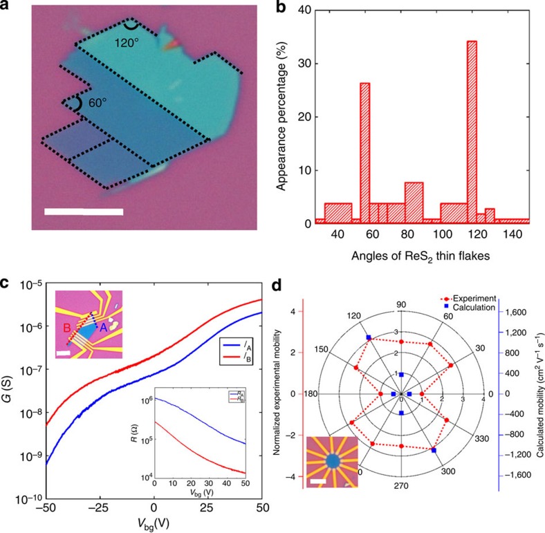
Figure 3. Anisotropic properties of ReS2.
(a) Optical image of a typical thin ReS2 flake with a quadrilateral shape. Scale bar, 5 μm. (b) The statistics of inner angles for over 20 thin ReS2 flakes, showing the greatest prevalence for 60° and 120°. (c) Transfer curves of anisotropic ReS2 FETs along two sides (A and B direction) of a quadrilateral-shaped five-layer flake (with an inner angle of 60° or 120°). Top inset: optical image of the devices. Scale bar, 10 μm. Low inset: the 4-probe resistance of the same devices with Vbg varying between 0 and 60 V. (d) Normalized field-effect mobility of a six-layer device along 12 directions evenly spaced at 30° apart plotted in polar coordinates (red dots with left axis). The direction with the lowest mobility was set to be the 0° (or 180°) reference. The optical image of the device is shown in the inset. The calculated mobility of monolayer ReS2 along three orientations (a axis, b axis and perpendicular to the a axis) is plotted in the same graph (blue dots with right axis) for comparison. The lowest mobility (a axis) direction was set to be the 0° (or 180°) reference as well.

