
Figure 1. The crystalline silicon-on-insulator (SOI) structure as seen by scanning electron microscope.
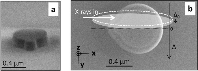
(a) Front view. (b) Same as (a), top view; The direction of the ptychography
translation  (black arrow) and the
scanning step
(black arrow) and the
scanning step  are indicated. The
projected direction of propagation of the incident beam (white arrow)
together with the beam footprint (FWHM of intensity, dotted ellipse) are
shown. The gray ellipse corresponds to the beam footprint at the next
beam-to-sample position. The (
are indicated. The
projected direction of propagation of the incident beam (white arrow)
together with the beam footprint (FWHM of intensity, dotted ellipse) are
shown. The gray ellipse corresponds to the beam footprint at the next
beam-to-sample position. The ( orthogonal laboratory frame is given.