
Figure 1.
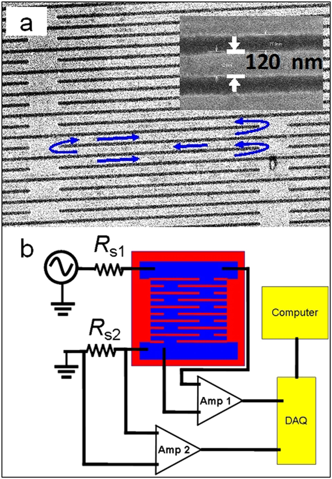
An SEM image of a niobium nitride photon detector and schematic diagram of the setup. (a) An SEM image of Sample 4. The NbN superconducting strip (lighter region) is roughly 250 μm in length and about 4 nm thick. The image is stretched vertically to make the strip more pronounced. The distance between the current turning points is about 7 μm, and the wide turns in the pattern allow the current to change direction without creating regions of high average current density. The path which the current travels is indicated by arrows. Not shown in the figure, to the far right or the far left, each horizontal NbN segment comes to an abrupt end and has no additional connections to the rest of the superconductor. The inset is a zoomed in view on one segment of the detector showing the width of the strip to be about 120 nm. (b) A schematic diagram of the setup. Superconducting NbN, shown in blue, is placed on a Si chip, which is shown in red. Voltage is measured directly across the sample. The voltage across  = 1 kΩ is used to determine the current though the strip using Ohm’s law. The resistor
  = 46 kΩ serves to limit the current in the circuit. Signals are amplified, read by a data acquisition (DAQ) card, and analyzed by computer.