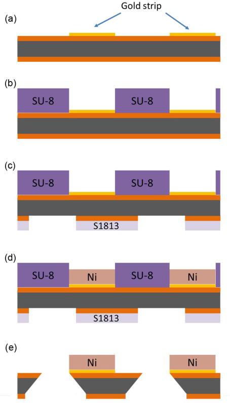
Fig. 2.

Side view of lid fabrication process flow. (a) Chrome/gold arrays were patterned onto double-side polished Si3N4 wafers using standard lithography techniques. The Si is shown in gray and the Si3N4 in orange (vertical dimensions not to scale). (b) SU-8 photoresist was patterned to define the shapes of electrodeposited Ni bars. (c) S1813 photoresist was patterned on the bottom of the wafer using back-side alignment, and the exposed silicon nitride was removed by reactive ion etching in CF4 to define a mask for wafer through-etching (d) Nickel bars were electrodeposited into the patterns established by the SU-8. (e) The wafer was etched in 30% w/v KOH at 130 C to create rectangular holes. Any remaining photoresist was removed by the KOH etch.
