
Fig. 3.
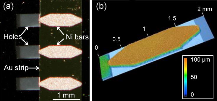
(a) Optical micrograph of a section of a lid array, showing three Ni bars, their underlying Au strip, and corresponding through-holes. The Ni bars appear bright due to reflected light from camera flash. The vertical-running edges of the Au strip are clearly seen, and the Si surface appears black. The holes appear gray due to the background below the wafer. (b) Height profile of a Ni bar, as indicated by the color scale. The thickness variation across the bar is < ± 2 μm. The bars’ dimensions were length L1 = 1.60 mm, width W1 = 450 μm, length of central rectangular section L2 = 775 μm, and tip width W2 = 90 μm. The region of the hole to the left of the bar appears in green due to an anomalous response of the optical profilometer to a region of that depth.