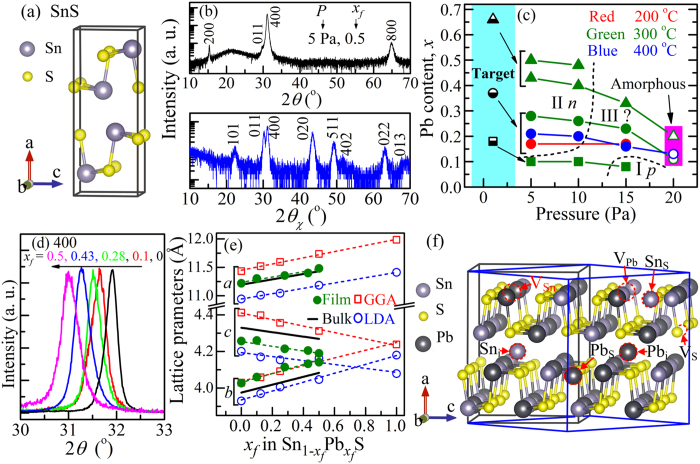
Figure 1. Structure of  films.
(a) Crystal structure of pure SnS. (b) Out-of-plane (top panel) and in-plane (bottom panel) synchronous scan XRD patterns of  film with xf = 0.5 grown at 300 °C and 5 Pa. (c) Pb content (xt for target, xf for thin films) as a function of pressure, substrate temperature, and xt. The half-filled symbols indicate the targets, the closed circles the orthorhombic phase crystalline films, and the open symbols amorphous films. (d) 400 out-of-plane XRD diffraction peaks of the
  films grown at 300 °C with various xf values. (e) Lattice parameters (a, b, c) of
  films as a function of xf. The closed circles indicate those obtained with the thin films, the solid lines are those of bulk (Sn1–xPbx)S taken from ref. 25, and the open symbols are the calculation results obtained by DFT in this work. The dashed straight lines are guides for eyes. (f) (Sn1-xPbx)S supercell model used for DFT calculations. The black line box draws the (Sn16–nPbn)S16 supercell model used for calculating the lattice parameters in Fig. 1e. The blue line box draws the (Sn16Pb16)S32 supercell model used for defect calculations in Fig. 4, where the intrinsic defect models examined in this study are indicated also in the figure.

