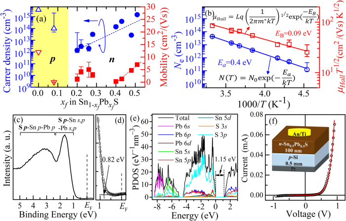
Figure 2. Electrical and electronic properties.
(a) Carrier density and mobility of  films as a function of xf measured by Hall effect. (b) Temperature dependences of electron density (Ne, blue line) and mobility (μe, red line) of n-type
  film with xf = 0.48. (c,d) UPS spectrum of n-type (Sn0.5Pb0.5)S film. (d) shows a magnified view near EF. (e) Projected DOS of (Sn0.5Pb0.5)S calculated by DFT with GGA functionals. (f) I-V characteristics of n-(Sn0.5Pb0.5)S/p-Si pn heterojunction. Inset shows the device structure.

