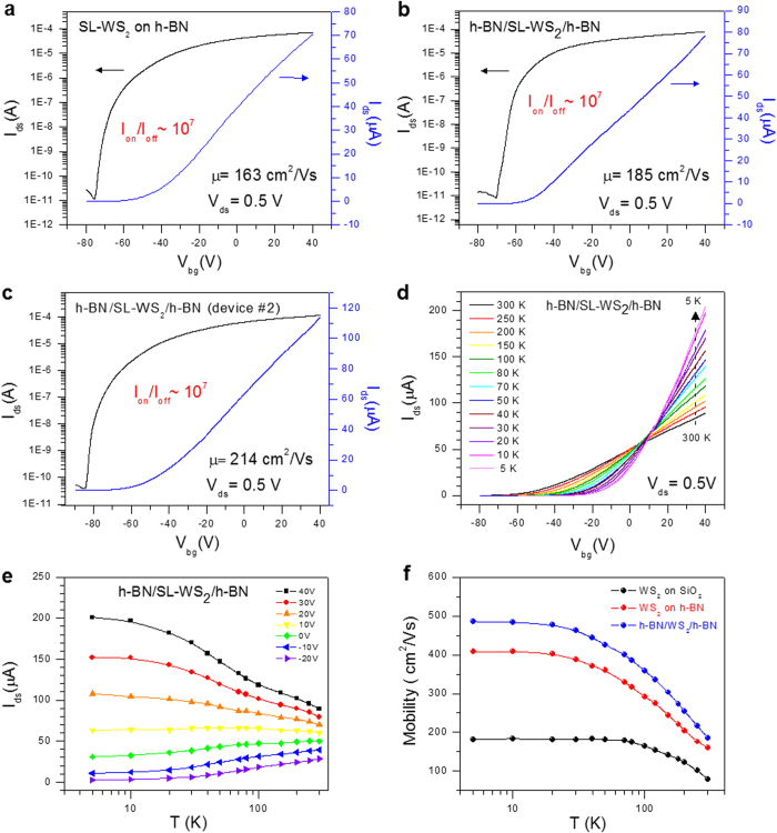
Figure 4. Transport properties of SL-WS2 FETs on CVD h-BN film.
(a) Transfer characteristics (Ids–Vbg) of the mechanically exfoliated SL-WS2 FET on CVD-grown h-BN film at 300 K. (b) Transfer characteristics (Ids–Vbg) of the mechanically exfoliated SL-WS2 FET enclosed by h-BN at 300 K. ON/OFF ratio of the device is ~107. (c) Transfer characteristics (Ids–Vbg) of the mechanically exfoliated SL-WS2 FET enclosed by h-BN (device #2) at 300 K. (d) Transfer characteristics (Ids–Vbg) of the mechanically exfoliated SL-WS2 FET enclosed by h-BN films at different temperatures. (e) Output current as function of temperature for different values of the back-gate voltage. (f) Electron field-effect mobility of SL-WS2 FETs on different substrates at various temperatures.

