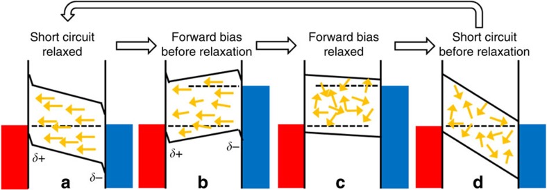
Figure 6. Consequence of polarized domain formation for device behaviour.
Schematic energy level diagram indicating the possible consequence of polarized domain formation in the presence of a built-in field on device behaviour. Yellow arrows indicate ferroelectric domain polarization direction, the dotted lines represent the Fermi or quasi-Fermi levels in the device and the solid lines represent the conduction and valence band energies. (a) Short circuit, equilibrium conditions. Ferroelectric domains have aligned to screen the built-in potential of the device. This reduces the strength of E-field in the bulk of the film, reducing the collection efficiency of any photo-generated charge carriers. (b) Under the application of a forward bias, the internal E-field is reduced or reversed, this allows the thermal randomization of the polarization directions. (c) Once the device has had time to relax to the forward bias conditions, there is little or no preferential orientation of ferroelectric domains. (d) When the device is returned to short circuit, the built-in potential is not screened by a net polarization direction of ferroelectric domains. This results in a stronger E-field in the bulk of the material and more efficient charge collection. The random domain alignment is gradually lost as the device relaxes back towards the equilibrium condition in a.

