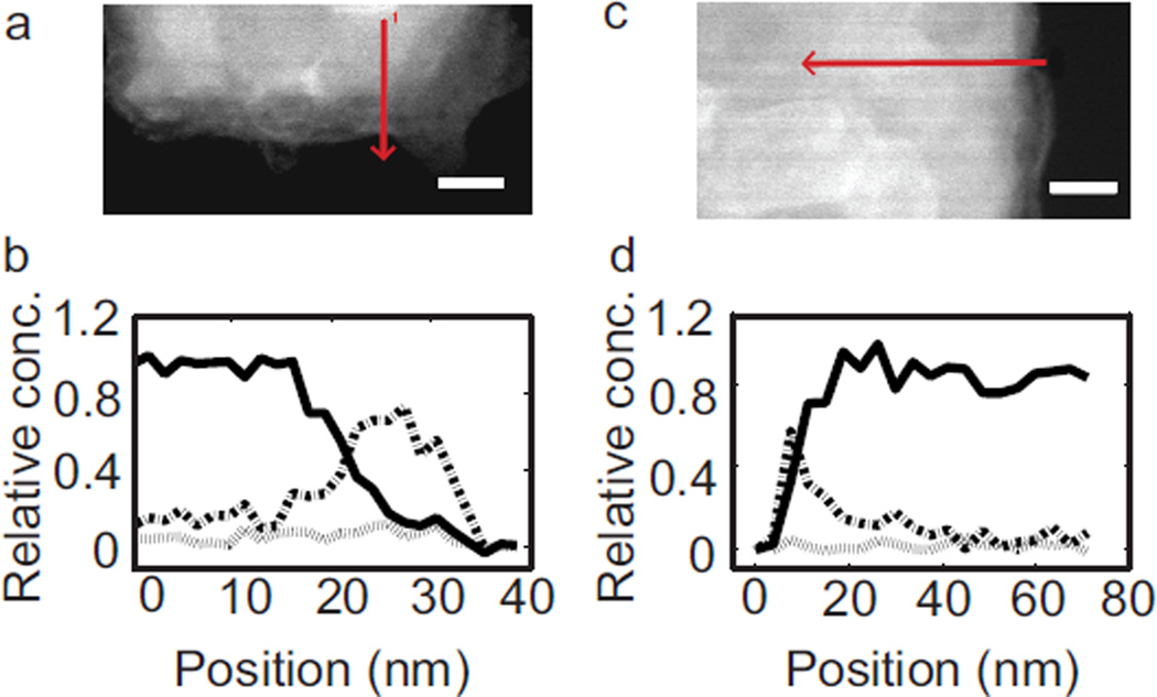
Figure 7.
Elemental mapping of an overhanging nickel nanorod by electron energy loss spectroscopy (EELS). Lines indicate the scanning direction. Leading edge (a) STEM image and (b) EELS signal. Side edge (c) STEM image and (d) EELS signal. The scale bars in (a) and (c) represent 20 nm. In the EELS scans of (b) and (d), nickel, oxygen, and chromium are plotted using solid, dot-dash, and dotted lines, respectively.

