Fig. 4.
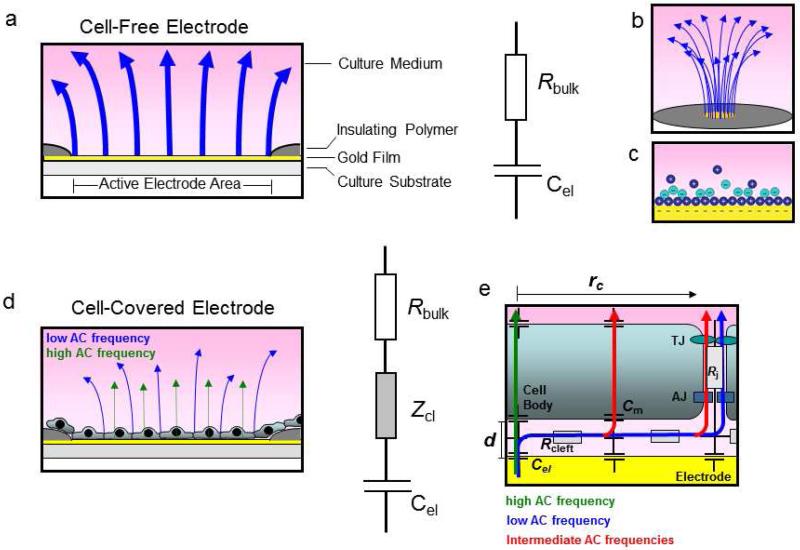
Schematic illustration of electrical behavior of a cell-free and cell-covered ECIS working electrode.a Schematic side view of a cell-free electrode and respective equivalent circuit presentation as resistor and capacitor in series. b Schematic presentation of electric compression of electric field lines (blue arrows) at the small opening of the working electrode. c Scheme of electrical double layer at a the electrode-solution interface. d Schematic side view of a cell-covered electrode, and respective equivalent circuit presentation which includes an additional impedance Zcl that arises from the cell layer. e Schematic presentation of AC current flow at the cell layer-electrode junction. Depending on AC frequencies, two different limiting cases of current flow across a cell layer consisting of cells with the radius rc in distance d above the electrode surface can be distinguished. At low frequencies the current takes the paracellular route (blue arrow) and takes up individual resistance contributions from the subcellular cleft (Rcleft) and the intercellular junctions (Rj). TJ: Tight junctions, AJ: Adherens junctions. At high frequencies the current couples capacitively across the membrane (green arrow). The impedance is dominated by the capacitance of the cell membrane (Cm). At intermediate frequencies current can take a varying combination of paracellular and transcellular routes (red arrows).

