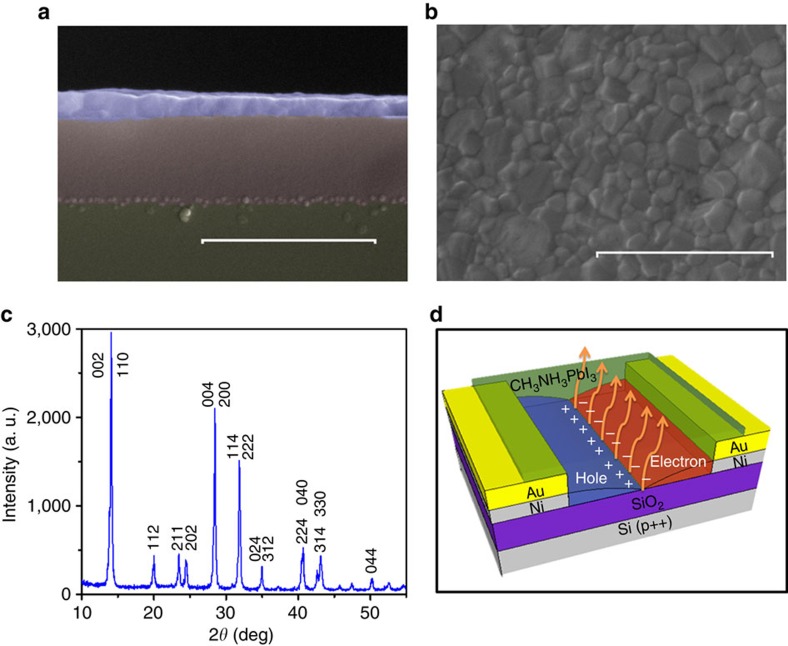
Figure 1. FET device configuration and thin-film characterization.
(a,b) Cross-sectional (a) and top-view (b) scanning electron miscroscope micrographs of the CH3NH3PbI3 thin film. Scale bars, 1 μm. (c) X-ray diffraction pattern of CH3NH3PbI3 film on SiO2/Si(p++) substrate, confirming the tetragonal structure of the perovskite and space group I4/mcm. (d) Schematic of the bottom-gate, bottom contact LE-FET configuration used in this study.

