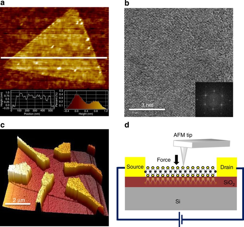
Figure 1. Characterization of the MoS2 monolayer and device structure.
(a) AFM image of a triangular MoS2 monolayer. Inset shows the histogram analyses of multiple topographic AFM images confirmed the MoS2 film thickness to be ∼0.75 nm. (b) High-resolution TEM image of the synthesized MoS2 monolayer. Inset is the corresponding diffraction pattern. (c) A typical AFM image of a MoS2 monolayer device. (d) Schematic illustration of a MoS2 device under mechanical load applied by an AFM tip.

