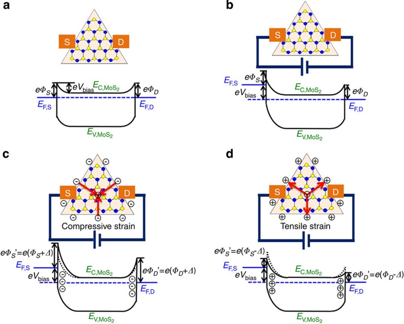
Figure 6. Band diagrams of the triangle monolayer MoS2 piezotronic device.
(a) Energy band diagram of the device without bias voltage. Schottky barrier has similar barrier heights at the S and D contacts. (b) Energy band diagram of the device with an external bias. The quasi-Fermi level is raised at the source contact. (c) Negative polarization charges induced on three zigzag edges of MoS2 under a local isotropic compressive strain, depleting free electrons near the contact interface and increasing the SBHs at both contacts. The asymmetry of band diagram is the result of the bias. (d) Positive polarization charges induced on three zigzag edges of MoS2 under a local isotropic tensile strain, attracting free electrons near the contact interface and decreasing the SBHs at both contacts. The red arrows represent the directions of polarization. EF is Fermi level of monolayer MoS2, EC is conduction band, EV is valence band, Vbias is the external bias and Δ is the piezopotential induced the change of barrier height.

