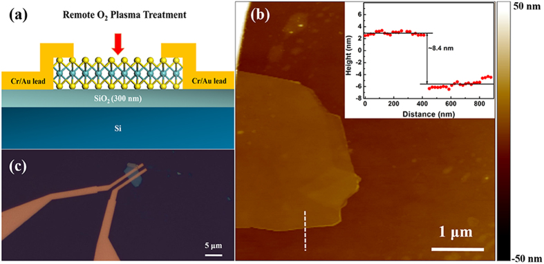
Figure 3. Fabrication of few-layer MoS2 transistors.

(a) Cross-sectional schematic of a back-gated MoS2 transistor treated with remote O2 plasma. (b) AFM image of a few- layer MoS2 flake on a 300-nm SiO2 substrate. The inset shows the cross-sectional plot along the white line in (b). (c) Optical image of the device using the flake in (b) as the channel. The substrate acts as a back gate. The channel length and width of the device are 1 and 4.2 μm, respectively.
