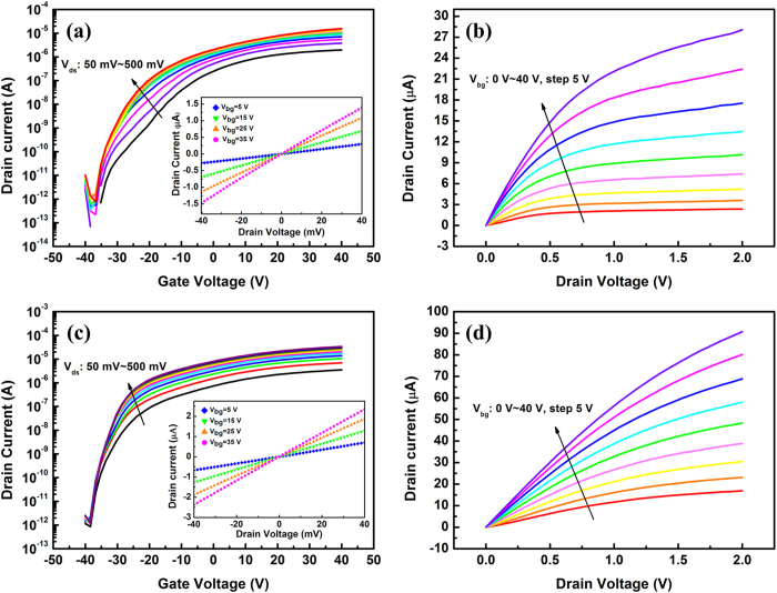
Figure 4. Electrical characterization of the few-layer MoS2 transistor.
(a,b) are the transfer and output characteristics for the original MoS2 transistor. (c,d) are the transfer and output curves for the same device after a 60 s remote O2 plasma treatment. The insets in (a) and (c) show the Ids–Vds curves with back-gate voltages of 5, 15, 25 and 35 V. The linear relationship between the current and voltage within −40 ~ 40 mV indicated that the Cr/Au electrodes form perfect ohmic contacts. All these curves were acquired at room temperature.

