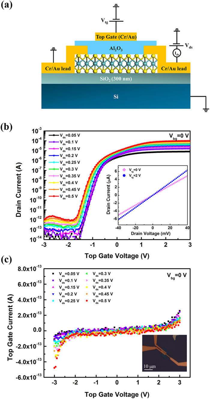
Figure 6. Top gate characteristics of a few-layer MoS2 transistor.

(a) Cross-sectional schematic of the top-gated devices together with the electrical connections. (b) Ids – Vtg curves with Vds ranging from 50 mV to 500 mV. The inset shows the Ids – Vds curves with the top gate voltages of 0 V and 2 V. (c) Top gate leakage current of the device. Optical image of the top gate device is attached as the inset of (c). Top gate dielectric of this device is 60 cycles Al2O3 deposited with 60 s remote oxygen plasma pretreatment. All these measurements were performed at room temperature with the back gate grounded.
