Abstract
Phonons, which are collective excitations in a lattice of atoms or molecules, play a major role in determining various physical properties of condensed matter, such as thermal and electrical conductivities. In particular, phonons in graphene interact strongly with electrons; however, unlike in usual metals, these interactions between phonons and massless Dirac fermions appear to mirror the rather complicated physics of those between light and relativistic electrons. Therefore, a fundamental understanding of the underlying physics through systematic studies of phonon interactions and excitations in graphene is crucial for realising graphene-based devices. In this study, we demonstrate that the local phonon properties of graphene can be controlled at the nanoscale by tuning the interaction strength between graphene and an underlying Pt substrate. Using scanning probe methods, we determine that the reduced interaction due to embedded Ar atoms facilitates electron–phonon excitations, further influencing phonon-assisted inelastic electron tunnelling.
 A fundamental understanding of electron–phonon interactions in graphene is crucial to developing graphene-based electronic and photonic devices. Here, the authors control the properties of phonons in graphene by tuning the interaction strength between graphene and an underlying platinum substrate.
Graphene, which is known to exhibit linear energy dispersion near the Fermi level, is considered a highly desirable material for future electronic1,2,3 and photonic4,5 devices owing to its unique electronic properties. The peculiar electronic band structure of graphene is markedly modified by many-body interactions6 such as electron–electron, electron–plasmon and electron–phonon interactions7,8. Phonons in graphene can be excited by tunnelling electrons from a tip through the use of scanning tunnelling microscopy (STM), and the electron–phonon coupling is revealed as an enhancement of electron tunnelling to graphene states with energies larger than the phonon energy. And these modifications manifest as a gap-like feature at the Fermi level in the tunnelling spectra obtained via scanning tunnelling spectroscopy measurements9,10,11,12. If controllable, therefore, phonons in graphene may present a valuable opportunity and play an integral role in graphene-based device applications, for example, as a ‘floodgate'9 of electronic current. However, very few studies have systematically explored the generation and control of phonons in graphene, and thus far, it has only been speculated that the phonon excitations may be influenced by the interaction between graphene and the underlying substrate10,11,12.
In the following, we propose a simple method to fabricate deformed graphene for easy modification of the graphene–substrate interaction with local control. We choose nanobubbles as the structural ‘knob', that is, an on-off switch for phonon control, and exploit the fact that noble-gas ions can penetrate below the first atomic layer of a graphite surface to form interstitial defects by low-energy impinging13,14,15.
Results
Formation of graphene nanobubbles
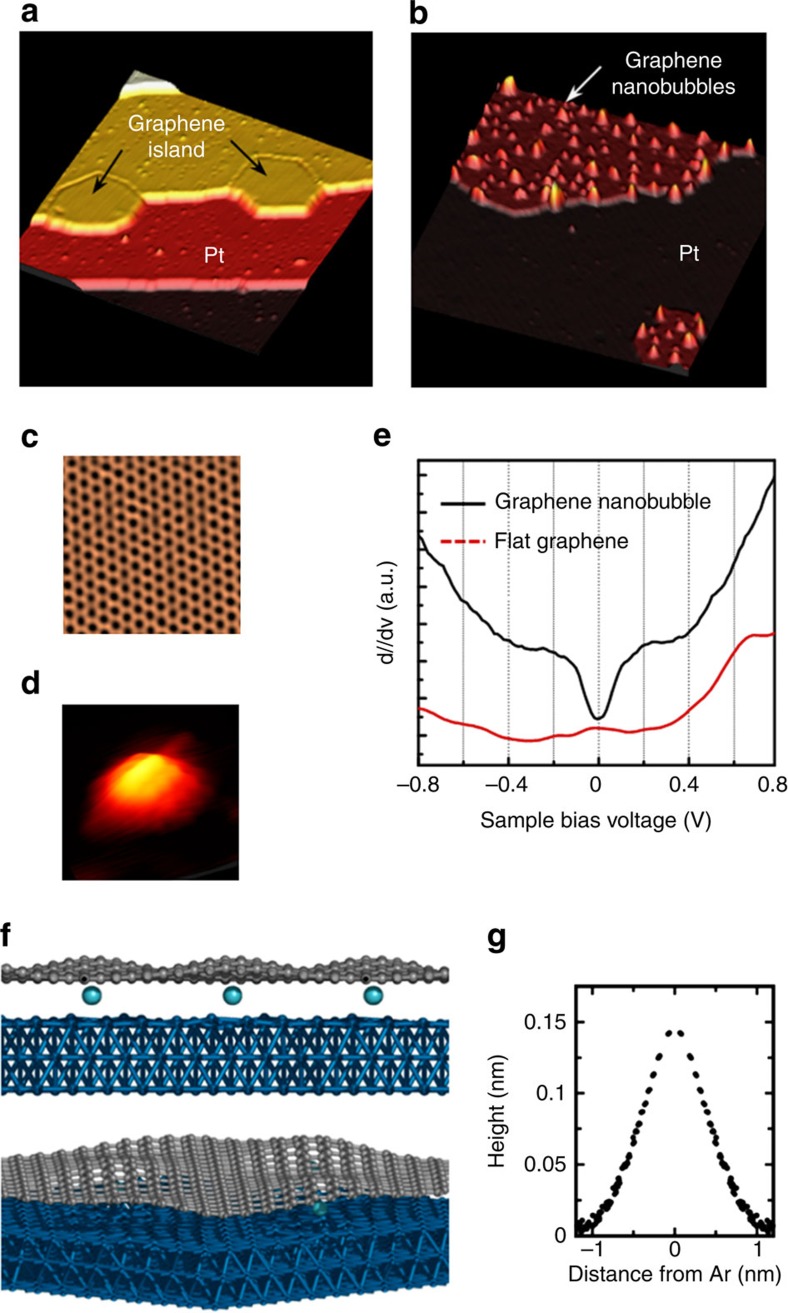
In our study, graphene nanoislands were first grown on a Pt(111) substrate. The large-scale topography (Fig. 1a) as well as the atomic-scale honeycomb lattice of graphene (Fig. 1c) was clearly observed via STM. On controlled irradiation by Ar+ ions, protrusions emerged as a result of certain modifications in graphene but not in Pt(111), as evident in Fig. 1b. The atomistic corrugation in the close-up STM topography (Fig. 1d) confirms changes in the structural and electronic properties in the irradiated graphene. The experimentally observed protrusions in the Ar+-ion irradiated graphene can in general be attributed to several origins such as adatom adsorption, vacancy-induced deformation16 and nanobubble formation by noble-gas-atom implantation13,14,15. In this context, we carefully eliminated the possibilities of adatoms and carbon vacancies as the reasons for the observed protrusions by controlling the energy and angle of Ar+-ion sputtering with subsequent annealing. This is evidenced by the fact that the generally observed resonance peak near the Dirac point, which is characteristic of vacancies in graphene, is indeed absent in the differential conductance (dI/dV) spectrum16 (Fig. 1e). Instead, the presence of the aforementioned gap-like feature near the Fermi energy clearly indicates that nanobubbles are selectively generated using our method. Density functional theory (DFT) calculation results also confirmed the structural deformation and the formation of nanobubbles in graphene on Ar-atom implantation between graphene and the Pt surface. As shown in Fig. 1f, graphene ‘bends' around the intercalated atoms and forms structures resembling the experimentally observed nanobubbles. With a single intercalated Ar atom, each nanobubble has approximate diameter and height of 2 nm and 0.15 nm, respectively (Fig. 1g), and these dimensions agree well with those of the smallest nanobubbles observed in our experiment. Our calculations also indicated that nanobubbles of various sizes can form with multiple Ar-atom implantations (see Supplementary Fig. 1).
Figure 1. Graphene nanobubbles on Pt(111).
(a) STM topograph of graphene nanoislands grown on Pt(111) (area of 50 × 50 nm2, Vs=0.5 V, It=0.5 nA). (b) STM topograph of graphene nanobubbles formed on graphene nanoislands (area of 25 × 25 nm2, Vs=0.5 V, It=1 nA). (c,d) Close-up STM topograph of the graphene honeycomb lattice (area of 2.8 × 2.8 nm2, Vs=0.4 V, It=30 nA) and nanobubble (area of 3.0 × 3.0 nm2, Vs=0.03 V, It=30 nA), respectively. (e) dI/dV spectra obtained at a graphene nanobubble (black line) and the flat graphene area (dotted red line). To make gap more evident, we added offset to the dI/dV spectrum measured in the flat graphene area. (f) Density functional theory (DFT)-optimized structure (side and tilted top views) of Ar-implanted graphene on Pt (111). The blue, grey and cyan spheres represent Pt, C and Ar atoms, respectively. (g) z-direction displacement of each C atom from a reference atom plotted against x–y-plane-projected distance from the closest Ar atom. The reference atom is selected to be the C atom closest to the Pt surface, and each point is duplicated for the corresponding negative distance.
Size dependence of nanobubbles in phonon excitations
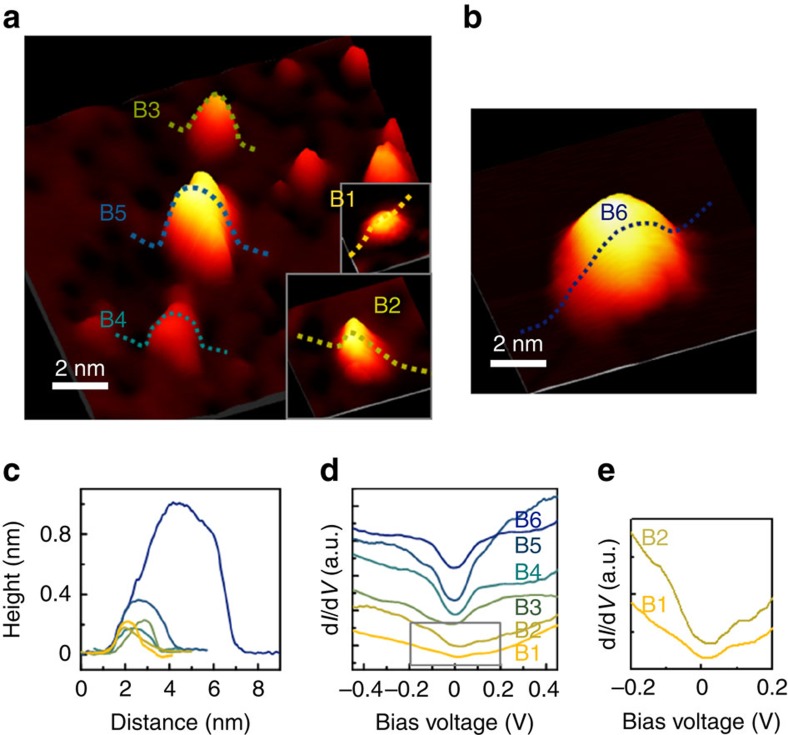
The bubbles labelled B1–B6 in Fig. 2a,b are representative examples of nanobubbles whose diameters and heights range from 1 to 6 nm and from 0.1 to 1.0 nm, respectively, as shown in the profiles (Fig. 2c) obtained along the dotted lines across B1–B6. The dI/dV spectra of the nanobubbles obtained near their apexes share the common gap-like feature centred at the Fermi level (Fig. 2d). While the ‘depth' of the gap and the slope of its edge increase monotonically with the size of the nanobubbles, the width and edge position of the gap exhibit no such dependence, which is further clearly evidenced by the magnified spectra of B1 and B2 in Fig. 2e.
Figure 2. STM topograph of various graphene nanobubbles and their corresponding differential conductance (dI/dV) spectra.
(a,b) STM topograph of graphene nanobubbles of various sizes. (Vs=50 mV, It=30 nA). (c) Dimensional cross-sections along the lines in a,b. (d) dI/dV spectra obtained at the centres of graphene bubbles B1–B6 shown in a,b. (e) Magnified dI/dV spectra near the Fermi level obtained at the centres of B1 and B2.
The gap-like feature in the dI/dV spectra signifies the suppression and/or enhancement of electron tunnelling at specific bias voltages, which we conclude to originate from phonon excitations. In graphene, out-of-plane phonons at K points in Brillouin zone can generate an inelastic tunnelling channel, and the structural nature of the nanobubbles facilitates such phonon excitations and mediates inelastic tunnelling. As a result, a gap-like feature emerges near the Fermi energy9,17. Since the momentum and energy of the excited phonons are fixed, the gap size must be independent of the nanobubble size, which in fact agrees with our experimental results. Here we remark that similar derivative features in the dI/dV spectrum may also result from nanobubble-induced curvature. Structural strain modifies the electronic structure of graphene rather substantially, as evident in the example of the strain-induced pseudo-magnetic field manifesting as Landau level peaks in the dI/dV spectrum11,18,19,20. However, the strain-induced changes in the electronic structure depend on the amount of the strain, specifically on the size of nanobubbles in our case. The degree of shift in the position of the Landau level peaks has indeed been reported to vary depending on the curvature11,19, which contradicts our observation. Changes in the dI/dV spectrum may also arise from the embedded Ar atoms, which can locally dope the graphene to cause a shift in the Dirac point21,22 or generate additional states to appear as peaks or dips in the tunnelling spectra. Such changes again must depend on the number of Ar atoms, or the size of the nanobubbles, which disagrees with our experiment. Our DFT calculations indeed did not show any discernible changes in the local density of states subsequent to the formation of nanobubbles, thus indicating that no additional charge states were present (See Supplementary Fig. 2).
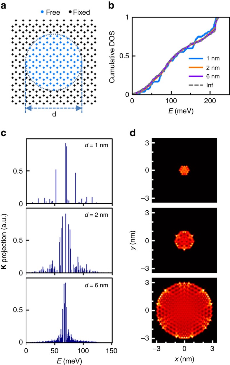
We examined how the lateral size of a graphene nanobubble influences phonon excitations via phonon-mode calculations by using an atomistic model. In our experiment, phonon excitations were localized in nanobubbles with diameters as small as 1 nm (B1, Fig. 2), so we constructed a simple model of a circular graphene dot (Fig. 3a), which mimics the case wherein the graphene is fully attached to the metal outside the dot while being completely free-standing inside the bubble. The complete phonon modes were computed for graphene dots with various diameters d, and the resulting normalized cumulative phonon density of states is shown in Fig. 3b. For all values of d, the cumulative phonon density of states exhibit nearly identical distributions although discrete jumps are observed in the case of d=1 nm because of the quantisation effect. Our results demonstrate that phonons are indeed excitable in nanobubbles with lateral sizes of ∼1 nm. The dependence of the phonon energy distribution on the bubble size was also explored by calculating the projection of each out-of-plane phonon mode to the plane wave with momentum K (K projection). As shown in Fig. 3c, the maximum value of K projection occurs at 68–70 meV for all finite-size dots, whose energy range corresponds well with the phonon energy of 67.3 meV in an infinite plane with momentum K. However, the larger the dot size is, the narrower the calculated distribution of the K projection becomes, and this behaviour explains why the depth and the edge slope of the gap-like feature in the dI/dV are observed to increase for larger bubbles. In addition, the calculation of the root mean square amplitude of the phonon modes (Fig. 3d) shows a uniform distribution for all nanodot sizes, which indicates that phonon signals are expected to be detected throughout the bubble. We note that the local variations in the amplitude result from the √3 × √3 pattern that is specific to the momentum K (see Supplementary Fig. 3).
Figure 3. Calculation of phonon modes in nanometre-size graphene dots.
(a) Schematic of graphene dot of diameter d, wherein the atoms inside the dot are free to move while those outside are stationary. (b) Graph of cumulative phonon density of states (DOS) for graphene dots with different diameters. All graphs are normalized so that the maximum cumulative phonon density of state (CDOS) is 1. (c) Projection of each phonon mode to a plane wave with momentum K and out-of-plane displacements for graphene dots with d=1, 2 and 6 nm. (d) Root mean square (r.m.s.) amplitudes of the phonon modes with K projections larger than one-third of the maximum K projection for the d values shown in c.
Spatial distribution of phonon excitations
To examine the spatial distribution of excited phonons around graphene nanobubbles, we obtained the spatial dI/dV maps and the corresponding numerical derivative (d2I/dV2) maps. The spatial dI/dV map in Fig. 4c and the corresponding d2I/dV2 map in Fig. 4d around nanobubble B6 (Fig. 2b and Fig. 4a) clearly indicate that phonon excitation only occurs within nanobubbles which are detached from the graphene. The nanobubble region becomes ‘dark' for energies in the range −70 to +70 meV in the dI/dV maps because of the gap, and a strong contrast is observed at around ±70 meV in the d2I/dV2 maps, which is manifested as a peak and dip in d2I/dV2 spectra in Fig. 4b. The boundary of the phonon excitation in the dI/dV and d2I/dV2 maps coincides with that of the nanobubble in the topograph. We also plotted the bias voltages of the largest peak in the d2I/dV2 spectra, Vph, shown in Fig. 4e, and the Vph shows little variation from 64 to 70 meV. However, the intensity of phonon signal increases as a function of the distance between the graphene and Pt layers, as plotted in Fig. 4f. The intensity increases by a factor of >2 when the separation between the Pt and graphene layers increases by 5 Å, which indicates that the phonon is more easily excited as the graphene–Pt interaction is reduced (see Supplementary Fig. 4). The exact mechanism by which the graphene–Pt interaction affects the phonon modes in nanobubbles are out of the scope of this paper; however, we note that the additional atomistic modelling demonstrates the phonon localization does occur by the change in the graphene–Pt interaction (see Supplementary Note 1, Supplementary Figs 5–7).
Figure 4. dI/dV and d2I/dV2 maps of nanobubble.
(a) STM topograph of graphene nanobubble B6 (Vs=500 mV, It=1 nA). (b) Averaged dI/dV (black) and d2I/dV2 (red) spectra. The d2I/dV2 spectra were calculated by numerical derivatives of the corresponding dI/dV spectra. The solid line indicates values obtained within the nanobubble, while the dotted line indicates values obtained for the outer flat region. Along the solid line, the bias values at which the maps were plotted in c,d are marked by dots. (c) dI/dV and (d) d2I/dV2 maps obtained over the area shown in a for bias voltages V=−131, −97, −64, −30, 3, 37, 104 and 138 mV from left to right. (e) Map of the bias voltage of the largest d2I/dV2 peak, Vph, which corresponds to the local phonon energy. (f) Map of the amplitude of d2I/dV2 values at Vph, [d2I/dV2]ph, which corresponds to the local phonon intensity.
Discussion
We successfully demonstrated phonon excitations in graphene via local control by generating nanobubbles of various sizes by means of Ar-ion irradiation. The reduced graphene–metal interactions due to Ar atoms embedded in between the graphene and metal substrate were shown to promote phonon excitations and enhance electron tunnelling above the phonon energy. We expect that our demonstrated control over phonon excitations down to the nanoscale will pave the way for advancements in graphene-based nano-electromechanical devices such as electrical switches based on the induced nonlinear I–V behaviour9. Our results also provide a fundamental understanding of the unwanted, yet possible, changes in electronic properties in actual graphene nanodevices, which arise from unwanted nanobubbles formed due to structural imperfections both in graphene and the supporting substrate.
Methods
Sample preparation and measurements
A Pt(111) sample was cleaned by means of repeated cycles of Ar-ion sputtering and annealing under ultrahigh vacuum. Graphene nanoislands were prepared by exposure of the clean Pt(111) surface to ethylene followed by annealing at 1,100 K23. To generate graphene nanobubbles, the graphene on the Pt(111) surface was irradiated with Ar+ ions (500 eV, 1 μA), and the sample was annealed at 1,000 K to remove additional impurities adsorbed onto graphene. Our STM measurements were performed using a Unisoku low-temperature STM at 2.8 K, and scanning tunnelling spectroscopy was performed using a conventional lock-in technique with a modulation bias voltage at a frequency of 1 kHz and an amplitude of 10 mV.
Modelling
Our first-principles calculations are based on the DFT employing the generalized gradient approximation with the projector-augmented-wave method as implemented in the Vienna ab initio simulation package24,25,26, and the electronic wave functions are expanded in a plane wave basis set with a cut-off energy of 273.9 eV. The vdW-DF2 (ref. 27) functional is also selectively employed. The periodically replicated system of a 9 × 9 graphene supercell placed on a three-layer slab of 8 × 8 Pt(111) with a vacuum spacing of ∼10 Å, which reproduced the experimentally observed moiré pattern, was first optimized. A part of the carbon atoms in graphene was subsequently manually deformed to introduce an Ar atom in between the graphene and the metal surface. The atomic positions of the resulting structure were relaxed until residual forces were <0.02 eV Å−1.
Atomistic calculation
We computed the Hessian matrix of the atoms within the graphene nanobubble using the adaptive intermolecular reactive empirical bond order (AIREBO) potential for carbon28, and we obtained the phonon spectra from the eigenvalues and eigenvectors of the Hessian matrix. We chose the AIREBO potential to avoid the otherwise large computational cost of first-principles calculations. While the phonon spectra from the AIREBO potential deviate slightly from the DFT calculations29, the AIREBO approach can correctly capture changes in the phonon spectra due to the boundary.
Additional information
How to cite this article: Kim, H.W. et al. Nanoscale control of phonon excitations in graphene. Nat. Commun. 6:7528 doi: 10.1038/ncomms8528 (2015).
Supplementary Material
Supplementary Figures 1-7, Supplementary Note 1 and Supplementary References
Acknowledgments
S.R. acknowledges the support of the Basic Science Research Program through the National Research Foundation of Korea (NRF) funded by the Ministry of Science, ICT & Future Planning (2013010091).
Footnotes
Author contributions H.W.K designed the experiments and performed the STM and STS measurements. H.W.K. and W.K. analysed the data. J.K., D.K. and S.R. carried out theoretical calculations. H.W.K., W.K. and J.Y.K. wrote the manuscript. All authors discussed the results and analysed the data.
References
- Yang H. et al. Graphene barristor, a triode device with a gate-controlled schottky barrier. Science 336, 1140–1143 (2012). [DOI] [PubMed] [Google Scholar]
- Zhang Y., Tan Y.-W., Stormer H. L. & Kim P. Experimental observation of the quantum Hall effect and Berry's phase in graphene. Nature 438, 201–204 (2005). [DOI] [PubMed] [Google Scholar]
- Li X. et al. Large-area synthesis of high-quality and uniform graphene films on copper foils. Science 324, 1312–1314 (2009). [DOI] [PubMed] [Google Scholar]
- Avouris P. Graphene: electronic and photonic properties and devices. Nano Lett. 10, 4285–4294 (2010). [DOI] [PubMed] [Google Scholar]
- Bonaccorso F., Sun Z., Hasan T. & Ferrari A. C. Graphene photonics and optoelectronics. Nat. Photonics 4, 611–622 (2010). [Google Scholar]
- Pisana S. et al. Breakdown of the adiabatic Born-Oppenheimer approximation in graphene. Nat. Mater. 6, 198–201 (2007). [DOI] [PubMed] [Google Scholar]
- Zhou S. Y., Gweon G. H. & Lanzara A. Low energy excitations in graphite: The role of dimensionality and lattice defects. Ann. Phys. 321, 1730–1746 (2006). [Google Scholar]
- Bostwick A., Ohta T., Seyller T., Horn K. & Rotenberg E. Quasiparticle dynamics in graphene. Nat. Phys. 3, 36–40 (2007). [Google Scholar]
- Zhang Y. et al. Giant phonon-induced conductance in scanning tunnelling spectroscopy of gate-tunable graphene. Nat. Phys. 4, 627–630 (2008). [Google Scholar]
- Sutter E., Acharya D. P., Sadowski J. T. & Sutter P. Scanning tunneling microscopy on epitaxial bilayer graphene on ruthenium (0001). Appl. Phys. Lett. 94, 133101 (2009). [Google Scholar]
- Levy N. et al. Strain-induced pseudo–magnetic fields greater than 300 tesla in graphene nanobubbles. Science 329, 544–547 (2010). [DOI] [PubMed] [Google Scholar]
- Gyamfi M., Eelbo T., Waśniowska M. & Wiesendanger R. Impact of intercalated cobalt on the electronic properties of graphene on Pt(111). Phys. Rev. B 85, 205434 (2012). [Google Scholar]
- Marton D., Boyd K. J., Lytle T. & Rabalais J. W. Near-threshold ion-induced defect production in graphite. Phys. Rev. B 48, 6757–6766 (1993). [DOI] [PubMed] [Google Scholar]
- Hahn J. R. & Kang H. Vacancy and interstitial defects at graphite surfaces: Scanning tunneling microscopic study of the structure, electronic property, and yield for ion-induced defect creation. Phys. Rev. B 60, 6007–6017 (1999). [Google Scholar]
- Cun H. et al. Immobilizing individual atoms beneath a corrugated single layer of boron nitride. Nano Lett. 13, 2098–2103 (2013). [DOI] [PubMed] [Google Scholar]
- Ugeda M. M. et al. Point defects on graphene on metals. Phys. Rev. Lett. 107, 116803 (2011). [DOI] [PubMed] [Google Scholar]
- Wehling T. O., Grigorenko I., Lichtenstein A. I. & Balatsky A. V. Phonon-mediated tunneling into graphene. Phys. Rev. Lett. 101, 216803 (2008). [DOI] [PubMed] [Google Scholar]
- Guinea F., Katsnelson M. I. & Geim A. K. Energy gaps and a zero-field quantum Hall effect in graphene by strain engineering. Nat. Phys. 6, 30–33 (2010). [Google Scholar]
- Lu J., Neto A. H. C. & Loh K. P. Transforming moiré blisters into geometric graphene nano-bubbles. Nat. Commun. 3, 823 (2012). [DOI] [PubMed] [Google Scholar]
- Kim H. W. et al. Strong interaction between graphene edge and metal revealed by scanning tunneling microscopy. Carbon NY 78, 190–195 (2014). [Google Scholar]
- Zhang Y., Brar V. W., Girit C., Zettl A. & Crommie M. F. Origin of spatial charge inhomogeneity in graphene. Nat. Phys. 5, 722–726 (2009). [Google Scholar]
- Deshpande A., Bao W., Miao F., Lau C. N. & LeRoy B. J. Spatially resolved spectroscopy of monolayer graphene on SiO2. Phys. Rev. B 79, 205411 (2009). [Google Scholar]
- Land T. A., Michely T., Behm R. J., Hemminger J. C. & Comsa G. STM investigation of single layer graphite structures produced on Pt(111) by hydrocarbon decomposition. Surf. Sci. 264, 261–270 (1992). [Google Scholar]
- Perdew J. P., Burke K. & Ernzerhof M. Generalized gradient approximation made simple. Phys. Rev. Lett. 77, 3865–3868 (1996). [DOI] [PubMed] [Google Scholar]
- Kresse G. & Furthmüller J. Efficient iterative schemes for ab initio total-energy calculations using a plane-wave basis set. Phys. Rev. B 54, 11169–11186 (1996). [DOI] [PubMed] [Google Scholar]
- Kresse G. & Joubert D. From ultrasoft pseudopotentials to the projector augmented-wave method. Phys. Rev. B 59, 1758–1775 (1999). [Google Scholar]
- Klimeš J., Bowler D. R. & Michaelides A. Van der Waals density functionals applied to solids. Phys. Rev. B 83, 195131 (2011). [Google Scholar]
- Stuart S. J., Tutein A. B. & Harrison J. A. A reactive potential for hydrocarbons with intermolecular interactions. J. Chem. Phys. 112, 6472–6486 (2000). [Google Scholar]
- Zhang H., Lee G. & Cho K. Thermal transport in graphene and effects of vacancy defects. Phys. Rev. B 84, 115460 (2011). [Google Scholar]
Associated Data
This section collects any data citations, data availability statements, or supplementary materials included in this article.
Supplementary Materials
Supplementary Figures 1-7, Supplementary Note 1 and Supplementary References


