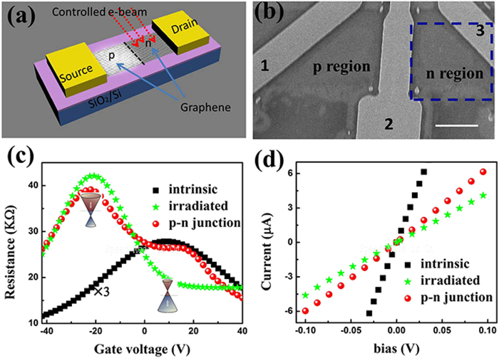
Figure 1. Device fabrication route and electrical characterizations.
(a) Schematic design of the electron irradiation modulated graphene field effect transistor (FET); (b) Scanning electron microscope (SEM) image of the electron irradiation graphene FET, and the squared area are marked for electron irradiation. The scale bar is 10 μm ; (c) The electric characteristics as a function of gate bias of the intrinsic graphene FET, the irradiated graphene FET and the fabricated graphene p-n junction; (d) Current-voltage (I-V) curves of the same sample in (a) at room temperature with zero gate bias. The black, blue and red color lines represent measurements between electrodes 1-2, electrodes 2- 3 and electrodes 1-3 as shown in Fig. 1(b), respectively.

