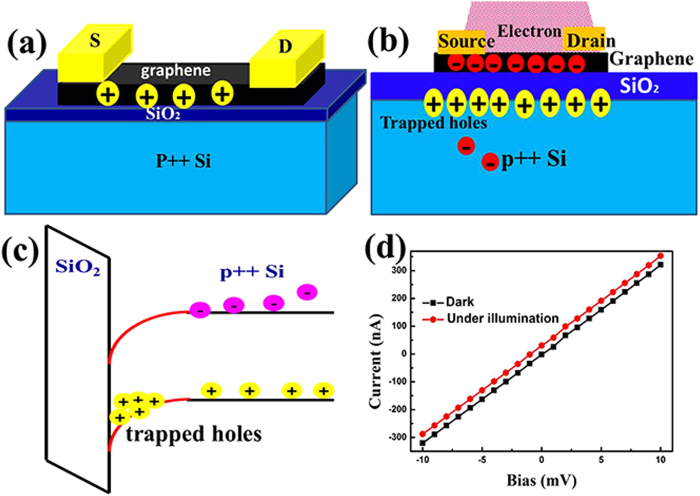
Figure 4. Substrate effect of electron irradiation.
(a) Schematic structure of the intrinsic p-type graphene FET device; (b) Substrate gating effect of the electron irradiation and charge distribution in the graphene FET on Si/SiO2 substrate; (c) Band diagram of Si/SiO2 interface, holes are trapped in the interface; (d) Id-Vd curve in the dark (black square) and under 633 nm laser illumination (red dot).

