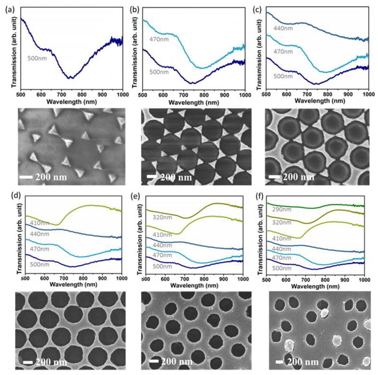
Figure 2. Correlation of optical and geometrical properties.

(a-f) The transmission and corresponding SEM image are shown for a nanohole array with periodicity of 500 nm and various etching times which cover the range of nanotriangle to nanohole to defect ridden pattern. The hole diameters from (a-f): 500 nm, 470 nm, 440 nm, 410 nm, 320 nm, and 290 nm. The defective pattern still has sufficient periodicity to support SPP and LSPR, albeit with a weakened response.
