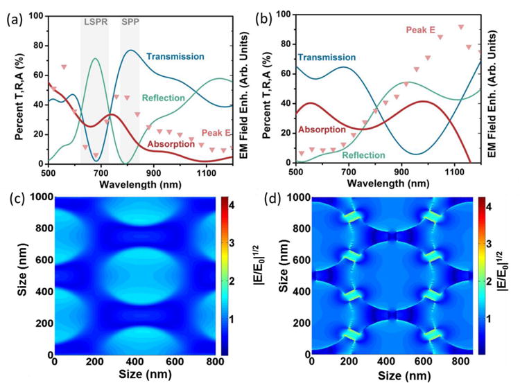
Figure 4. Comparison of optical modes and resulting EM field enhancement for 500 nm periodicity.

The transmission (T), reflection (R), and absorption (A=1-T-R) is compared to the peak EM field enhancement for an (a) ordered and (b) ‘gap’ defective pattern. For the ‘gap’ defect, the EM field from an ordered and defective pattern of the same hole size are shown for comparison. The absorption and EM field are similar for the ordered pattern, with the local field (c) focused on the nanohole walls, but differ (d) for the defective pattern, with the local field focused within and at the ‘gap’ defect edges. (a) and (c) are the data of ordered Au nanohole array with a periodicity or 500 nm, a hole diameter of 350 nm, and a film thickness of 50 nm; (b) and (d) are the data of Au nanohole array of the same parameter as (a) and (c) but with 50 nm ‘gap’ defects.
