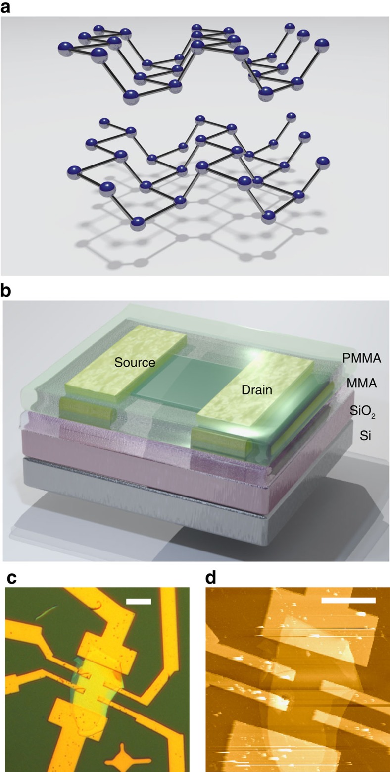
Figure 1. Structure of black phosphorus FETs.
(a) The bP crystal structure is composed of puckered honeycomb layers with an interlayer distance of 5.24 Å. (b) Three-dimensional schematic view of a bP FET with oxidized silicon back-gate and an encapsulating layer of MMA and PMMA. (c) Optical image of an encapsulated bP FET in Hall bar geometry. Scale bar, 10 μm. (d) AFM image of the same device with encapsulating layer removed. The bP thickness is 43±2 nm (82±4 atomic layers). Scale bar, 10 μm.

