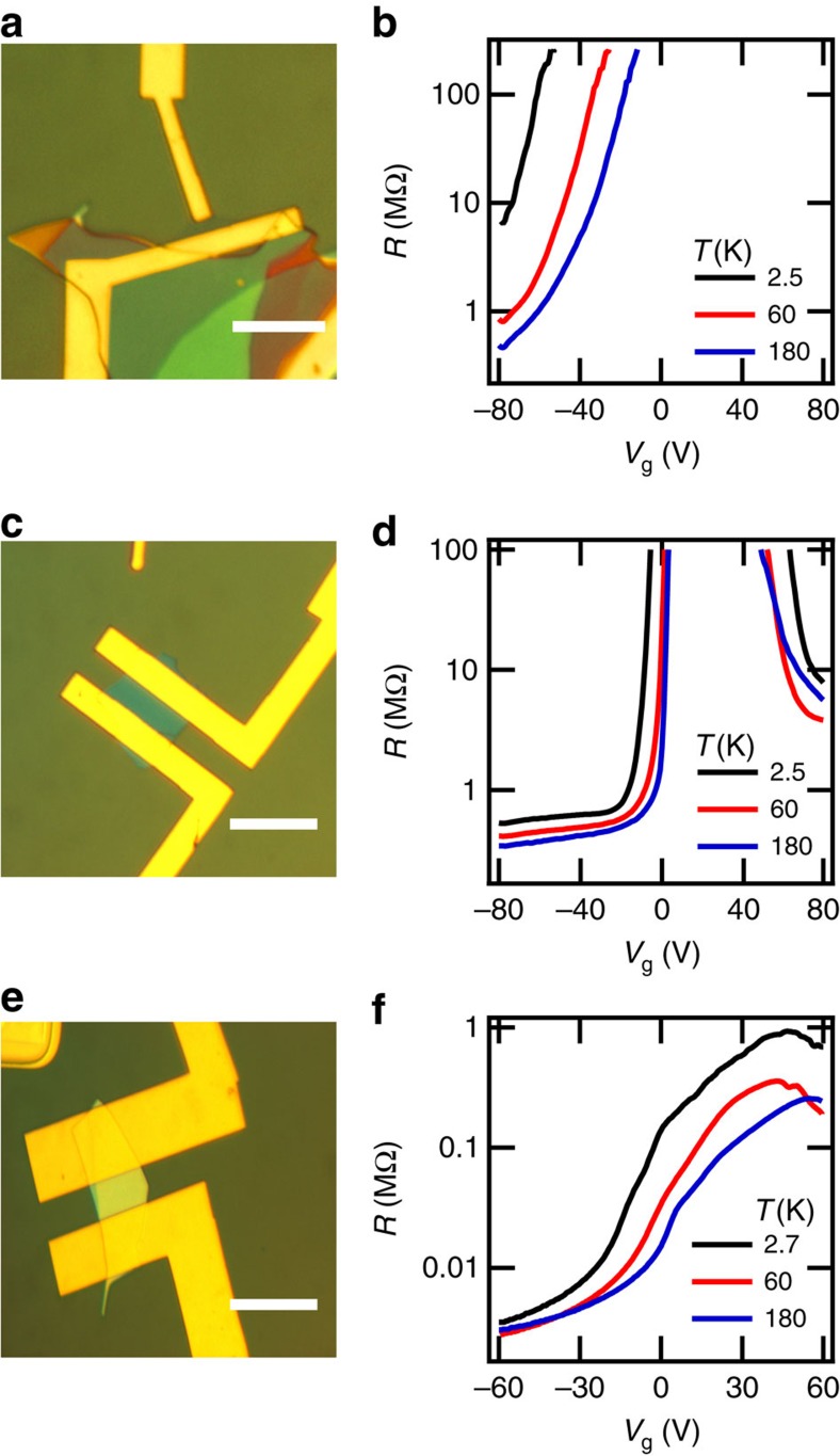
Figure 2. Black phosphorus FET characterization.
(a,c,e) Optical images of encapsulated devices with increasing thickness of 6±1 nm, 12.5±1 nm and 47±1 nm, respectively. Scale bar, 5 μm. (b,d,f) Source-drain resistance R as a function of gate voltage Vg measured with an ac source-drain bias at different temperatures for the devices shown in a,c,e, respectively. The thickest 47±1 nm device exhibits a resistance two orders of magnitude smaller than the devices of thickness 12.5±1 nm and 6±1 nm.

