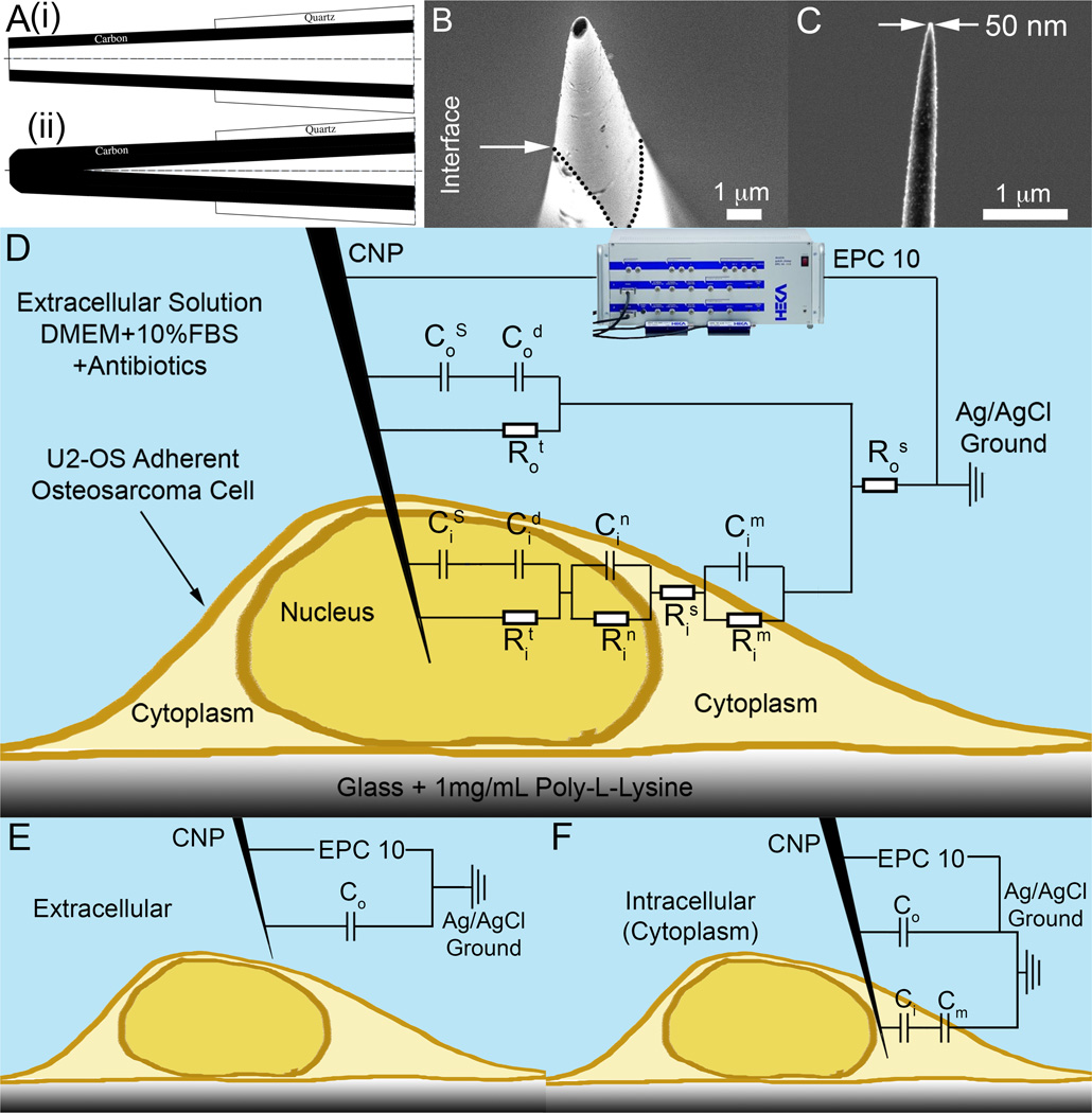
Figure 1.
Carbon Nanopipettes (CNPs) for cell probing. (A) A schematic depiction of the CNP’s cross-section. (i) Open-tipped (hollow) CNP. (ii) Solid CNP. (B) A SEM side micrograph of a CNP’s tip (500nm diameter, inclined at 10° off-axis). The quartz-carbon interface is delineated with dotted lines. (C) A SEM side view of a solid CNP with 50nm tip diameter. (D–F) A schematic depiction of a CNP penetrating an adherent cell with the equivalent circuit model overlaid. C and R denote, respectively, capacitors and resistors. Subscripts o, and i designate, respectively, extracellular and intracellular circuit components. Superscripts designate the following: S - Stern layer (capacitance), s- series (resistance), d – diffuse layer, n – nuclear membrane, m – cellular membrane, t – charge transfer. When modeling cytoplasm probing, the nuclear circuit elements (Cin and Rin) are omitted. (D) Complete circuit model. (E) Extracellular circuit approximation, only capacitors are included. (F) Intracellular (cytoplasm) circuit approximation, only capacitors are included.

