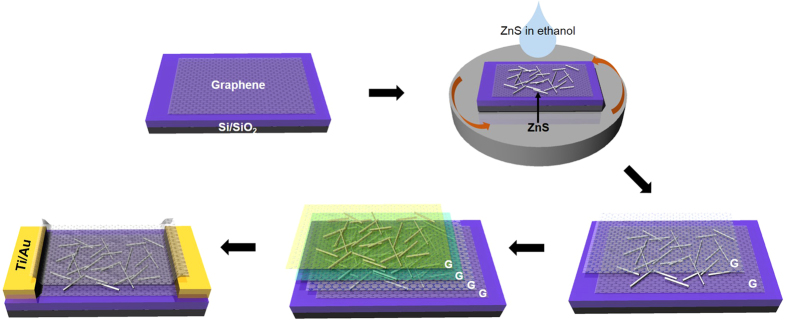
Figure 1. Schematic for the fabrication of a G/ZnS device.

(a) graphene transfer, (b) ZnS spin coating, (c) graphene stacking, (d) repeated b and c steps for multiple coating and stacking, and (e) device fabrication with metal electrodes.

(a) graphene transfer, (b) ZnS spin coating, (c) graphene stacking, (d) repeated b and c steps for multiple coating and stacking, and (e) device fabrication with metal electrodes.