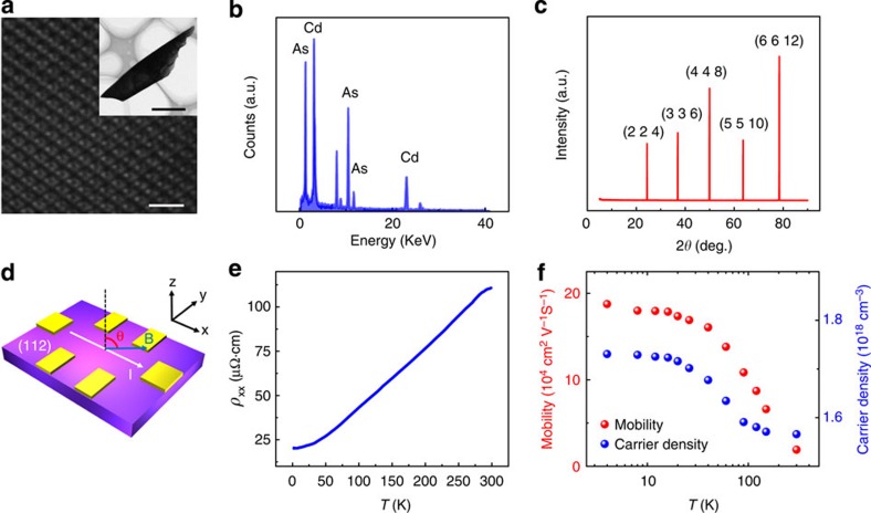
Figure 1. Structural and electrical properties of Cd3As2 bulk crystals.
(a) A high-resolution TEM image of a Cd3As2 thin flake on a holey carbon grid, revealing a perfect crystalline structure. Inset is a low magnification TEM picture. The white and black scale bars correspond to 2 nm and 1 μm, respectively. (b) A typical EDX spectrum showing the atomic ratio of Cd:As=3:2. (c) X-ray diffraction patterns of the single crystal Cd3As2. The peak position shows that the sample surface is in {112} planes. (d) A constant current was applied within the {112} atomic planes while the magnetic field was titled in the x–z plane, as depicted by the blue arrow. (e) The longitudinal resistivity ρxx as a function of temperature, showing a typical metallic behaviour. (f) The temperature-dependent mobility and carrier density from 2.6 to 300 K. At 2.6 K, the mobility reaches 1.9 × 105 cm2 V−1 s−1.

