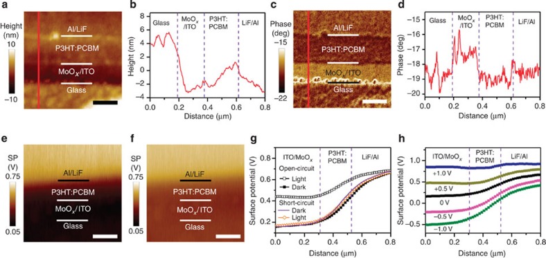
Figure 2. Cross-sectional images and depth profiles of a BHJ device.
(a) Topography and (c) phase images of the ITO/MoOx/P3HT:PCBM/LiF/Al device cross-section obtained with AFM (scale bars, 200 nm). The line profiles in b,d correspond to the red lines in a,c, respectively. SP images of the P3HT:PCBM BHJ device in open-circuit (e) in the dark and (f) under AM 1.5G illumination (scale bar, 250 nm); (g) SP depth profiles of the device in open-circuit in the dark (solid black squares), in open-circuit under AM 1.5 G illumination (open black squares), in short-circuit in the dark (solid purple line) and in short-circuit under AM 1.5 G illumination (open orange diamonds); (h) SP depth profiles of the P3HT:PCBM BHJ device in the dark with bias voltages ranging from −1.0 to +1.0 V. The wiring configuration for applying the bias voltage is illustrated in Fig. 1b.

