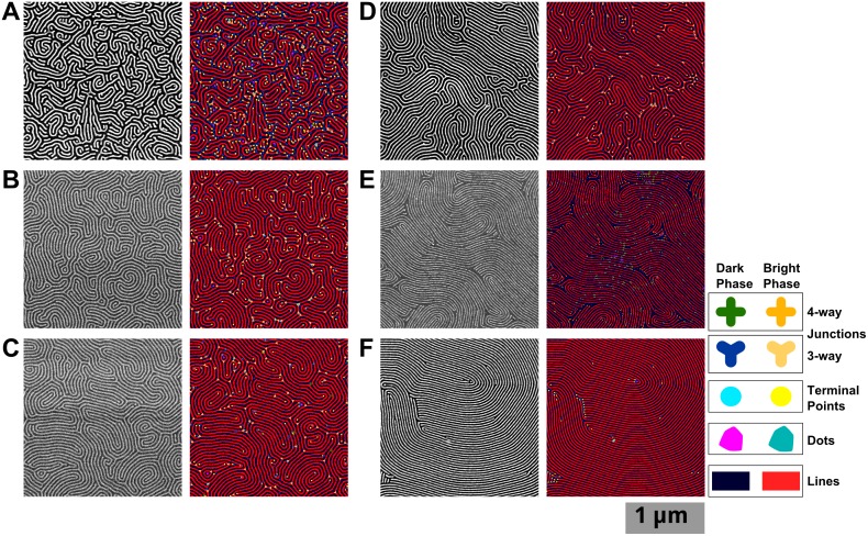
Fig 13. Original and defect analysis images for six SEM images of metallized PS-b-P2VP (50k-b-16.5k, 44k-b-18.5k, and 32.5k-b-12k) patterns with different degrees of thermal annealing.
SEM images on left, and confirmation images with defects identified shown right. These images are spectacular only upon a close-up. Each image is shown cropped here to ~2 μm wide. The scale bar is 1 μm. (See S5 Fig for full images). The labels (A-F) show correspondence to the same processed images in Fig 12.

